Printed circuit board and manufacturing methods of printed circuit board and plate hole of printed circuit board

A technology of printed circuit board and manufacturing method, which is applied in printed circuit manufacturing, printed circuit, printed circuit and other directions, can solve the problems of decreased hole position accuracy, large copper thickness, poor uniformity of surface copper thickness, etc., and achieves convenient and fast manufacturing. The effect of thin surface copper thickness and high hole position accuracy

Active Publication Date: 2015-02-11
NEW FOUNDER HLDG DEV LLC +1
View PDF6 Cites 13 Cited by
  • Summary
  • Abstract
  • Description
  • Claims
  • Application Information

AI Technical Summary

Problems solved by technology

[0004] However, the inventors found that this method needs to be drilled twice, the accuracy of the hole location will decrease, and it needs to be electroplated and plugged twice, which leads to poor uniformity of surface copper thickness and large copper thickness, which is not conducive to the production of high-density fine lines

Method used


Image

  • Printed circuit board and manufacturing methods of printed circuit board and plate hole of printed circuit board
  • Printed circuit board and manufacturing methods of printed circuit board and plate hole of printed circuit board
  • Printed circuit board and manufacturing methods of printed circuit board and plate hole of printed circuit board

Examples


Embodiment 1

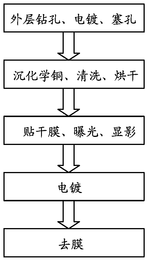
[0037] The manufacturing method of the holes in the PCB in this embodiment is applicable to the manufacturing of PCBs with isolated holes in the board without connection. After plugging all the holes, carry out copper sinking, and then use dry film to cover the places that do not need to be made into the hole in the plate and need to control the thickness of the copper on the surface, and then remove the dry film after electroplating, and the partial hole in the plate can be completed. .

[0038] The specific process is as follows:

[0039] (1) Drill, electroplate, and plug all the holes on the outer layer of the PCB;

[0040] It should be noted that in this process, the thickness of thin copper plating can be controlled between 18um and 25um;

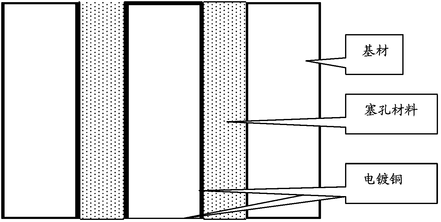
[0041] figure 2 It is the effect diagram of using resin plug holes for all the hole diameters that need to be plugged in the first implementation of the present invention; it is best to polish the slightly convex part of the hole a...

Embodiment 2

[0057] The manufacturing method of the PCB hole in this embodiment is applicable to the manufacture of a PCB in which the hole in the board is not isolated but connected (that is, the hole in the board is connected to other circuit PAD (soldering point)). For local electroplating, it is necessary to make holes in the plate. After the copper thickness is sufficient, this part of the hole is plugged, and then copper plating is performed to plug the remaining holes, and the partial hole in the plate can be completed. The specific process is as follows:

[0058] (1) Drill out all the holes on the outer layer of the printed board, and electroplate thin copper (5-8um);

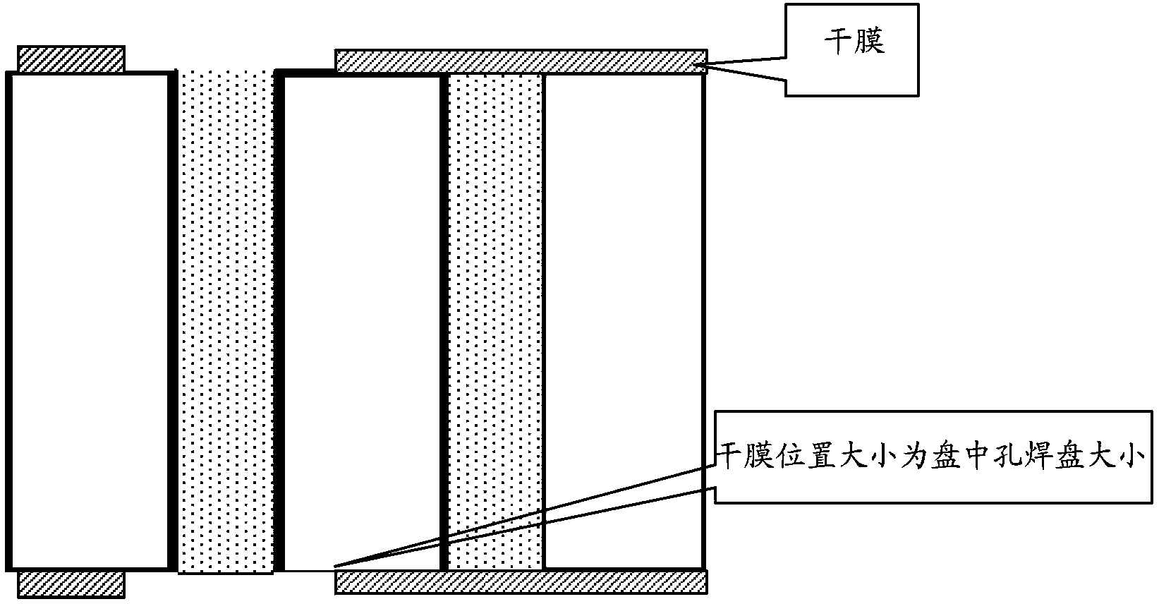
[0059] (2) Applying dry film, exposure, and development;

[0060] Only the locations where holes in the disc need to be made are developed. Preferably, the exposed size of the development is slightly smaller than the size of the holes in the disk, for example, 50um smaller on one side, so as to ensure the alignmen...


PUM


Abstract

The invention discloses a manufacturing method for a plate hole of a printed circuit board (PCB). The method includes the following steps: drilling an outer-layer hole, which includes a plate hole, of the printed circuit board; carrying out copper deposition on the drilled outer-layer hole and an outer-layer board; pasting a dry film on the outer-layer board and adopting exposure and development to remove the dry film at the position of the plate hole; and carrying out electroplating on the printed circuit board after development to remove the dry film after the development. Through use of the method, manufacturing of the PCB is convenient and rapid and the hole position precision is high and the thickness of surface copper is low and the printed circuit board is suitable for manufacturing high-density fine circuits.

Description

technical field [0001] The present invention relates to the technical field of PCB (Printed Circuit Board, printed circuit board), in particular to a printed circuit board and a method for manufacturing the printed circuit board and the hole in the plate. Background technique [0002] The hole in the plate is an important part of the multilayer PCB. From the perspective of function, the hole in the plate can be divided into two categories: one is used for the electrical connection between layers; the other is used for fixing or positioning the device. In terms of process, these holes in the disk include blind vias and through vias. Blind holes are located on the top and bottom surfaces of the PCB and have a certain depth for the connection between the surface circuit and the underlying inner circuit. The depth and diameter of the hole usually do not exceed a certain ratio. Through holes pass through the entire circuit board and can be used for internal interconnection or as...

Claims


Application Information

Patent Timeline
Patent Type & Authority Applications(China)
IPC IPC(8): H05K1/11H05K3/40
CPCH05K1/113H05K1/116H05K3/425H05K2201/0959
Inventor 黄世清李金鸿陈显任
Owner NEW FOUNDER HLDG DEV LLC
Why Eureka
Try Eureka