CMOS (Complementary Metal Oxide Semiconductor) low-temperature low-noise operational amplifier circuit

An operational amplifier circuit and low-noise technology, applied in the field of CMOS low-temperature and low-noise operational amplifier circuits, can solve problems such as the inability to apply mainstream CMOS circuit design, no adoption, etc., achieve high power supply voltage suppression ratio, overcome circuit oscillation, reduce effect of noise

Inactive Publication Date: 2015-02-18
SHANGHAI INST OF TECHNICAL PHYSICS - CHINESE ACAD OF SCI
View PDF1 Cites 12 Cited by
  • Summary
  • Abstract
  • Description
  • Claims
  • Application Information

AI Technical Summary

Problems solved by technology

[0003] The Chinese patent CN 1588794 A of Cao Bisong et al., authorized on March 2, 2005, announced a low-temperature low-noise amplifier in the radio frequency band. The amplifier belongs to the field of radio frequency technology and is mainly used in the CDMA band. process, does not use the current conventional CMOS process, and cannot be applied to the design of current mainstream CMOS circuits

Method used


Image

  • CMOS (Complementary Metal Oxide Semiconductor) low-temperature low-noise operational amplifier circuit
  • CMOS (Complementary Metal Oxide Semiconductor) low-temperature low-noise operational amplifier circuit
  • CMOS (Complementary Metal Oxide Semiconductor) low-temperature low-noise operational amplifier circuit

Examples


Embodiment 1

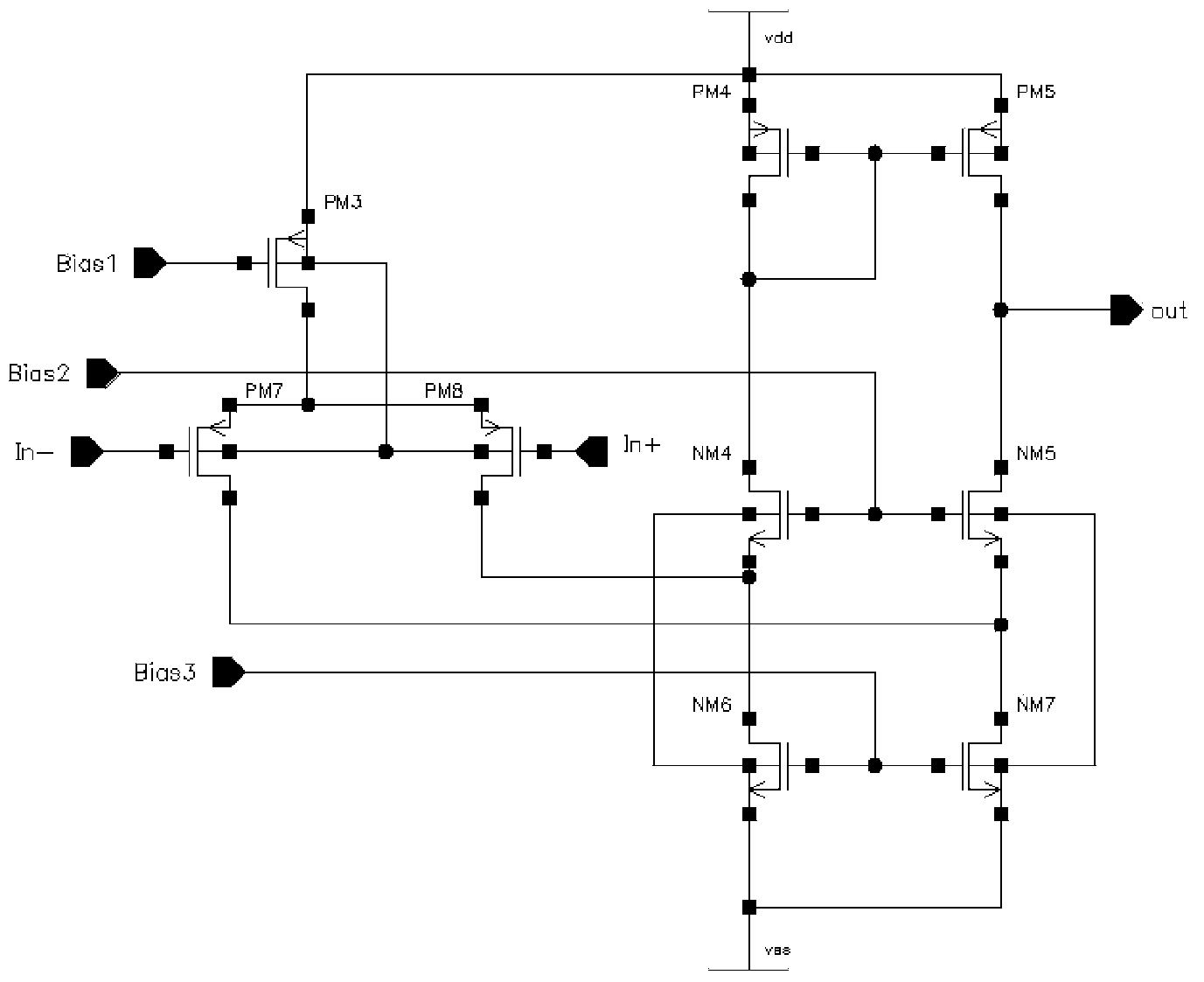
[0020] The total noise of this circuit is mainly determined by the input tubes PM7 and PM8, and the equivalent input noise voltage calculation formula is:

[0021] S v e ( f ) = 8 3 kT g m + K f C ox 2 WL 1 f (in g m = 2 K p W L I ds )

[0022] The first term is channel thermal noise and the second term is 1 / f noise.

[0023] g m For the transconductance of the input ...

Embodiment 2

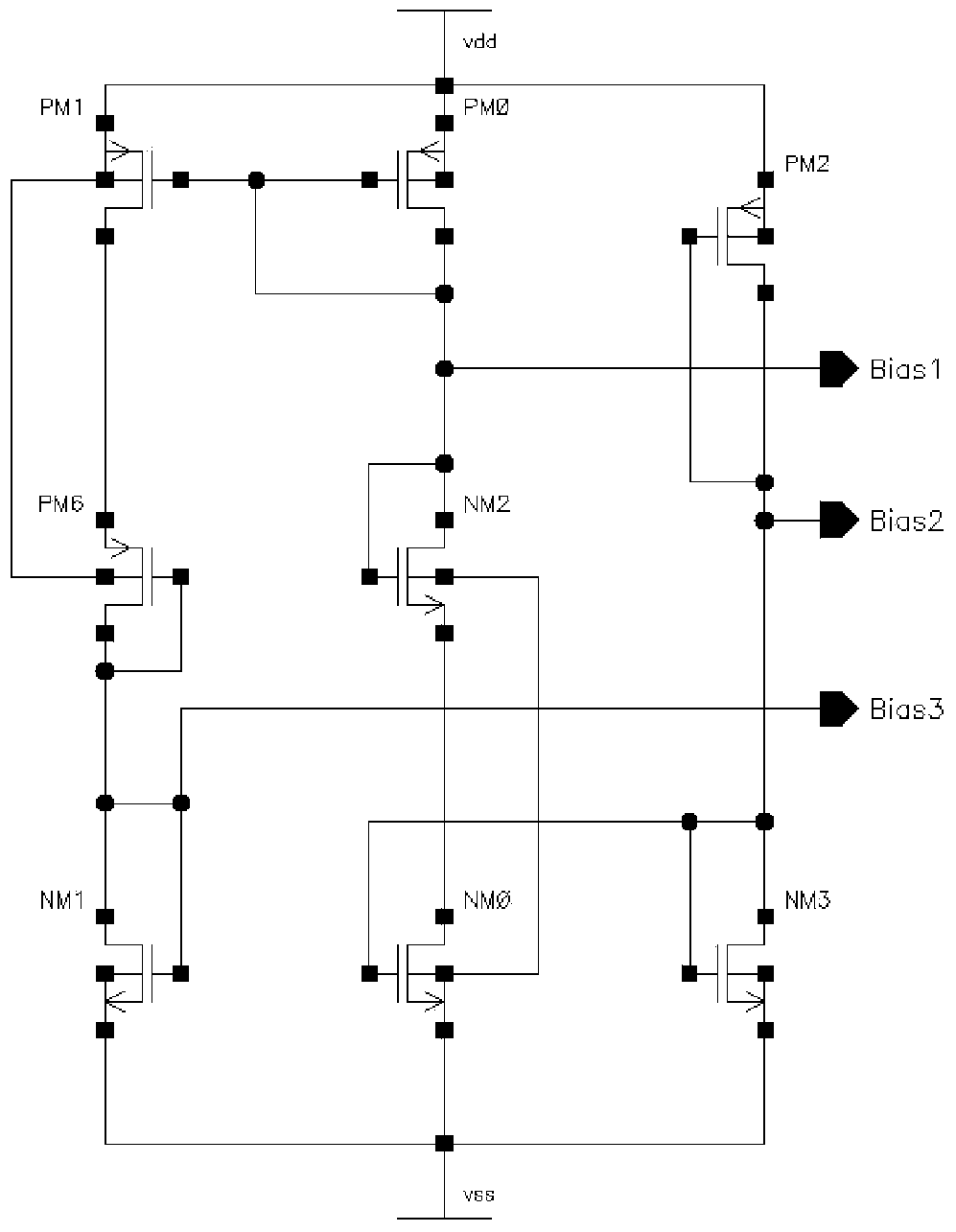
[0027] The bias circuit section of this low temperature low noise CMOS differential operational amplifier is as figure 2 As shown, NM3 and NM0 constitute the first-stage current mirror, PM0 and PM1 constitute the second-stage current mirror, NM1 and the NM6 and NM7 of the enlarged part constitute the current mirror, and PM0 and the PM3 of the enlarged part constitute the current mirror.

[0028] The bias part is composed of eight tubes. PM2 and NM3 connected by diodes form a reference current source. NM3 is mirrored to NM0 to generate one current, and then PM0 is mirrored to PM1 to generate another current. This current source does not use the pair Passive resistors that are particularly sensitive to temperature, so the current source can work normally at room temperature and low temperature. The test results show that the current source has a strong temperature suppression ability, so the entire low-temperature CMOS differential operational amplifier chip has a wide operating...

Embodiment 3

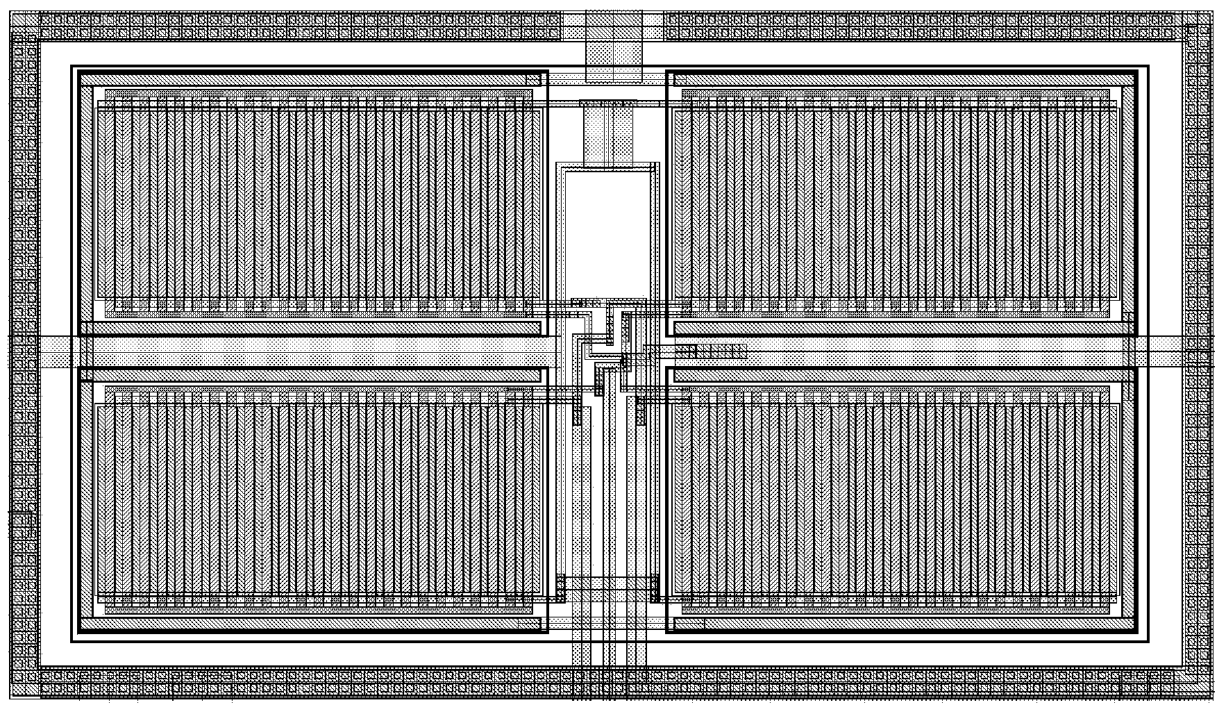
[0032] When drawing the layout of the amplifier, all pairs of tubes use interdigitated transistors, and try to ensure up-down and left-right symmetry, which can reduce the input offset of the CMOS differential operational amplifier at low temperature, especially the input tube of the differential amplifier, which is particularly important. In this circuit, since the differential input pair tube uses a large tube of 1500μm / 1.5μm, in order to achieve up-down and left-right symmetry, 72 41.7μm / 1.5μm tubes are used to form the input pair tube when drawing the layout, as shown in image 3 As shown, this greatly reduces the input offset of the entire differential operational amplifier, and the test results show that the input offset voltage of the low-temperature low-noise CMOS differential operational amplifier is very small, less than 1mV.


PUM


Abstract

The invention discloses a CMOS (Complementary Metal Oxide Semiconductor) low-temperature low-noise operational amplifier circuit. A biasing circuit part adopts a multi-stage current mirror sleeving mode, and reference current is generated by an active resistor of an MOS (Metal Oxide Semiconductor) tube comprising two connected diodes, so that the reference current of an amplifier has better temperature characteristics; an amplification part is of a differential input folded cascode structure, the open loop gain of the amplifier can be greater than 80dB by virtue of one-stage amplification, and the defect that oscillation is easily caused by a Miller compensation capacitor used by the conventional two-stage amplification at the low temperature of 77K is overcome; a large tube of which the width to length ratio is greater than 100 is adopted for differential input, the noise performance of a CMOS amplifier is improved favorably, and a differential operational amplifier can normally work at the normal temperature and the low temperature of 77K, can be used as a standard amplifier module designed for a low-temperature CMOS circuit, can be applied to a photovoltaic infrared detector circuit, and can also be applied to a long-wave infrared optical guide detector circuit.

Description

technical field [0001] The invention relates to a CMOS operational amplifier circuit, in particular to a CMOS low-temperature and low-noise operational amplifier circuit. Background technique [0002] In the field of aerospace remote sensing, most infrared detectors work at low temperature. In order to improve the performance of the system and reduce the interference introduced by the outside world, it is required that the detector be connected to the circuit at close range, that is, the designed circuit also needs to work at low temperature. Currently, commercialized circuit products are designed for room temperature and may not work properly at low temperatures. In order to improve the performance of the system, it is necessary to design a CMOS readout circuit that can work normally at low temperature. The core module of the readout circuit is a CMOS differential operational amplifier. If there is a mature low-temperature CMOS differential operational amplifier module, it ...

Claims


Application Information

Patent Timeline
IPC IPC(8): H03F3/45H03F1/26H03F1/30
CPCH03F1/26H03F1/301H03F3/45192H03F2200/372H03F2203/45054
Inventor 袁红辉陈永平陈世军宋伟清
Owner SHANGHAI INST OF TECHNICAL PHYSICS - CHINESE ACAD OF SCI
Why Eureka
Try Eureka