A Diffusion Method of Buffer Layer

A diffusion method and buffer layer technology, applied in electrical components, semiconductor/solid-state device manufacturing, circuits, etc., can solve the problems of difficult control of parameter influence, long advancing diffusion time, and low efficiency, achieving low cost and short advancing diffusion time. , the effect of high efficacy

Active Publication Date: 2017-03-22
HUBEI TECH SEMICON
View PDF4 Cites 0 Cited by
  • Summary
  • Abstract
  • Description
  • Claims
  • Application Information

AI Technical Summary

Problems solved by technology

Due to the special equipment required for ion implantation and the long time of propulsion and diffusion, the cost of ion implantation is high and the efficiency is low, and the long-term high-temperature propulsion has a great impact on other parameters and is difficult to control

Method used


Image

  • A Diffusion Method of Buffer Layer
  • A Diffusion Method of Buffer Layer
  • A Diffusion Method of Buffer Layer

Examples


Embodiment Construction

[0029] In order to make the above objects, features and advantages of the present invention more comprehensible, specific implementations of the present invention will be described in more detail below in conjunction with the accompanying drawings.

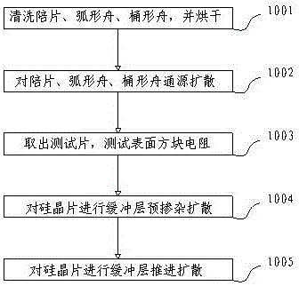
[0030] figure 1 The schematic flowchart shown includes step 1001, step 1002, step 1003, step 1004 and step 1005, which are described in detail as follows.

[0031] Step 1001: Cleaning multiple companion wafers, multiple silicon wafers, arc boats and barrel boats.

[0032] According to the conventional cleaning process, clean multiple accompanying sheets, arc-shaped boats, and barrel-shaped boats. The accompanying sheets and arc-shaped boats are made of conventional N-type single crystal or quartz materials, and the barrel-shaped boats are made of conventional N-type single crystal, polycrystalline, or quartz materials. kind of. If the companion piece is of quartz material, a test piece of silicon material shall be prepared; if t...


PUM


Abstract

The invention provides a buffer layer diffusion method, belongs to the technical field of semiconductor manufacture, and is mainly to solve the problems of high cost, low efficiency, very large influence on other parameters and difficult control in the preparation of a buffer layer through ion implantation and high-temperature propulsion mode at present. The buffer layer diffusion method is mainly characterized in that the method comprises the following steps: cleansing and drying a bucket boat, an arc boat, test wafers and silicon wafers; putting the bucket boat, the arc boat, and the test wafers into a diffusion tube for carrying out source-pass doped diffusion to enable the surfaces thereof to be respectively accumulated with a layer of uniform impurity atoms; cleansing and drying the bucket boat, the arc boat, and the test wafers above, and arranging the test wafers and the silicon wafers in a manner that one test wafer and two silicon wafers are in lamination arrangement; putting the bucket boat, the arc boat, the test wafers and the silicon wafers into a diffusion furnace tube for high-temperature pre-diffusion; and taking out the silicon wafers and putting the silicon wafers on the arc boat, and then putting the arc boat into a high-temperature diffusion furnace for carrying out buffer layer propulsion diffusion. The buffer layer diffusion method has the advantages that an existing common processing line can realize buffer layer diffusion, low cost, short propulsion diffusion time, and the effect of not being influenced by types of impurities, and the method is mainly used for buffer layer diffusion of a power semiconductor device chip.

Description

technical field [0001] The invention belongs to the technical field of semiconductor manufacturing. The invention relates to a buffer layer diffusion method of a power semiconductor device chip. Specifically, it is a buffer layer phosphorus or aluminum atom transfer diffusion method. Background technique [0002] With the development of semiconductor device manufacturing technology, the requirements for devices such as high voltage, high current, and low voltage drop are also getting higher and higher. To meet the demand, buffer layer technology is introduced in semiconductor manufacturing technology. [0003] Since the buffer layer requires a relatively shallow concentration and a certain junction depth, the gas-carrying source diffusion method of the existing common process has a high concentration, so it is difficult for the gas-carrying source diffusion method to reach the shallow concentration required by the buffer layer. For this reason, the current buffer layer di...

Claims


Application Information

Patent Timeline
Patent Type & Authority Patents(China)
IPC IPC(8): H01L21/22
CPCH01L21/2205
Inventor 刘小俐张桥颜家圣杨宁
Owner HUBEI TECH SEMICON
Why Eureka
Try Eureka