Optical pumping white-light LED and preparation method thereof
An optical pumping and LED chip technology, applied in the field of white LEDs, can solve the problems of large color shift, less red and green light components, and increased response time, and achieve the effects of long service life, satisfactory light efficiency, and short response time.
- Summary
- Abstract
- Description
- Claims
- Application Information
AI Technical Summary
Problems solved by technology
Method used
Image
Examples
no. 1 example
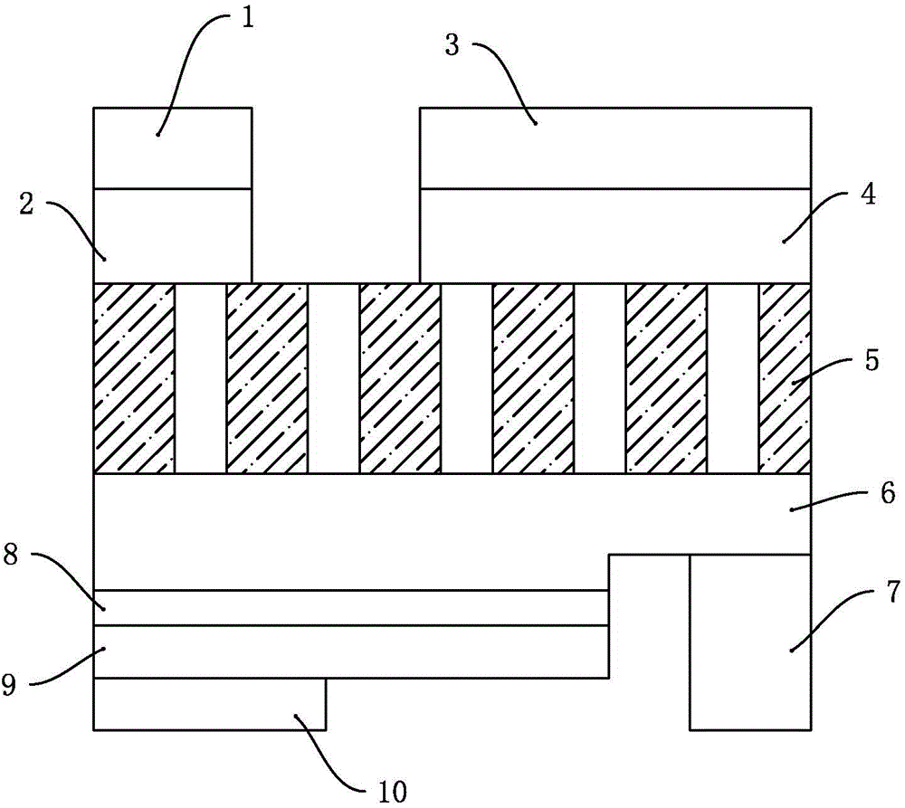
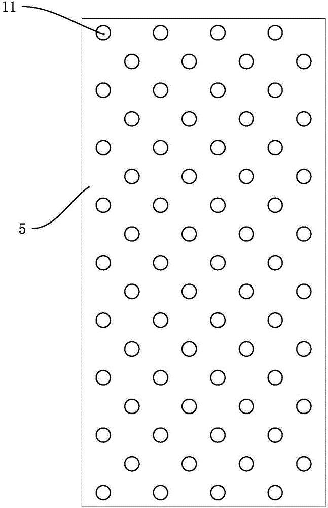
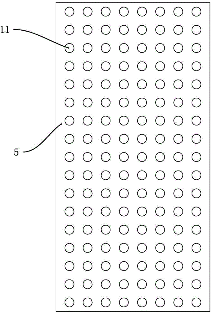
[0030] Such as Figure 1 to Figure 4 As shown, an optically pumped white LED includes a planar blue LED chip, and the planar blue LED chip includes a sapphire substrate 5, an n-type GaN layer 6, an InGaN / AlGaN double heterojunction layer 8, and a P-type GaN layer 9; P-type GaN layer 9 is provided with P electrode 10, and n-type GaN layer 6 is provided with n-electrode 7; The upper surface of sapphire substrate 5 has a photonic crystal array that makes blue light emit to the vertical direction of sapphire substrate 5 , one side of the upper surface of the photonic crystal array is sequentially provided with a red band DBR layer 2 and a red band AlGaInP epitaxial layer 1 from bottom to top, and the other side of the upper surface of the photonic crystal array is sequentially provided with a green band DBR layer from bottom to top 4 and AlGaInP epitaxial layer 3 in the green band. One side of the surface of the photonic crystal array is provided with a red-band AlGaInP epitaxial...
no. 2 example
[0038] A method for preparing an optically pumped white light LED, comprising the following steps:
[0039] (1) Prepare planar blue LED chips according to the MOCVD method; obtained by metal organic chemical vapor deposition MOCVD (Metal Organic Chemical Vapor Deposition) growth technology, the substrate is sapphire, and the growth process uses hydrogen (H 2 ) and nitrogen (N 2 ) as carrier gas, the Ga source, In source and N source used are trimethylgallium (TMGa), trimethylindium (TMIn) and ammonia (NH 3 ), the p-type dopant and n-type dopant used are magnesium dicene (Cp 2 Mg) and silane (SiH 4 ).
[0040] (2) Remove impurities on the surface of the sapphire substrate. The sapphire substrate undergoes high-temperature heat treatment in the reaction chamber to remove surface impurities. First, a 25-35nm low-temperature (730°C) GaN buffer layer is grown on the sapphire substrate, and the temperature rises (1150°C) to grow 1.5 ~3.0um unintentionally doped GaN semiconductor...
PUM
 Abstract
Description
Claims
Application Information
 - R&D
- Intellectual Property
- Life Sciences
- Materials
- Tech Scout
- Unparalleled Data Quality
- Higher Quality Content
- 60% Fewer Hallucinations
Browse by: Latest US Patents, China's latest patents, Technical Efficacy Thesaurus, Application Domain, Technology Topic, Popular Technical Reports.
© 2025 PatSnap. All rights reserved.Legal|Privacy policy|Modern Slavery Act Transparency Statement|Sitemap|About US| Contact US: help@patsnap.com


