Wafer-level packaging method for a semiconductor device

A wafer-level packaging and semiconductor technology, used in semiconductor devices, electrical components, circuits, etc., can solve the problem of large differences in mechanical properties between phosphor layers and substrates, cracking and breaking of photodiode packaging products, and limiting the space for packaging light sources, etc. problem, to achieve the effect of easy holding, easy processing, and reducing thermal stress

Active Publication Date: 2017-05-31
JIANGYIN CHANGDIAN ADVANCED PACKAGING CO LTD
View PDF1 Cites 0 Cited by
  • Summary
  • Abstract
  • Description
  • Claims
  • Application Information

AI Technical Summary

Problems solved by technology

like figure 1 As shown, the traditional photodiode uses expensive sapphire or silicon carbide as the substrate to form a photodiode chip, which limits the space for reducing the production cost of the photodiode, and its thickness is generally above 500 microns, which limits the space for packaging the light source; At the same time, the mechanical properties of the phosphor layer and the substrate of the white light photodiode are quite different, and thermal stress is easily formed due to temperature changes during the process or use, which leads to cracking and breaking of the photodiode packaging product, reducing product reliability. sex

Method used


Image

  • Wafer-level packaging method for a semiconductor device
  • Wafer-level packaging method for a semiconductor device
  • Wafer-level packaging method for a semiconductor device

Examples


Embodiment Construction

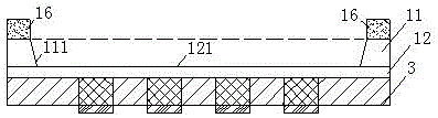
[0050] see figure 2 , the technological process of the wafer-level packaging method of a semiconductor device of the present invention is as follows:

[0051] S101: Take a silicon wafer, on which an epitaxial layer is grown on the silicon substrate;

[0052] S102: forming an array of metal bumps on the surface of the epitaxial layer, encapsulating them, and thinning them to expose the surface of the other end of the metal bumps;

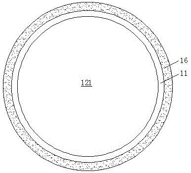
[0053] S103: Thinning the silicon substrate, removing the middle region of the silicon substrate to expose the light-emitting surface of the epitaxial layer;

[0054] S104: Divide the epitaxial layer, and sequentially form a phosphor layer and a light-transmitting layer on the epitaxial layer;

[0055] S105: cutting the silicon wafer that has completed the packaging process into packages of individual semiconductor devices.

[0056] The present invention will now be described more fully hereinafter with reference to the accompanying drawings, in ...


PUM


Abstract

The invention relates to a wafer level package method for a semiconductor device, and belongs to the technical field of semiconductor package. The wafer level package method includes the process flows: providing a silicon-based wafer; forming an arrayed metal projection on the surface of an epitaxial layer of the silicon-based wafer through a projection process; packaging the metal projection, thinning a packaging layer and exposing the surface of the metal projection; turning over and thinning the other surface of a silicon substrate; removing a light-exiting surface of a middle area of the silicon substrate exposed to the epitaxial layer by the aid of an annular reticle mask or jig, and processing the microstructure of the exposed light-exiting surface of the epitaxial layer; dividing the epitaxial layer into crisscross epitaxial layer intervals; forming a fluorescent powder layer and an euphotic layer in an annular cavity; cutting the silicon-based wafer along the epitaxial layer intervals to form an independent single photodiode. The photodiode package method is thin, small in stress and low in cost.

Description

technical field [0001] The invention relates to a wafer-level packaging method for a semiconductor device, belonging to the technical field of semiconductor packaging. Background technique [0002] Photodiodes, semiconductor devices that convert electricity into light, have come a long way as a new source of solid-state lighting. Due to the influence of factors such as product performance, manufacturing cost, and external dimensions, the packaging forms of photodiodes are also constantly evolving and enriching: traditional photodiode packaging forms mainly include bracket-type packaging, plastic-encapsulation-type EMC packaging, and metal printed board-type COB packages, and ceramic substrate-style packages. Such as figure 1 As shown, the traditional photodiode uses expensive sapphire or silicon carbide as the substrate to form a photodiode chip, which limits the space for reducing the production cost of the photodiode, and its thickness is generally above 500 microns, whi...

Claims


Application Information

Patent Timeline
Patent Type & Authority Patents(China)
IPC IPC(8): H01L33/50H01L33/52H01L33/62
CPCH01L33/005H01L33/502H01L33/52H01L33/54H01L33/62H01L2933/0041H01L2933/005
Inventor 陈栋张黎陈海杰陈锦辉赖志明
Owner JIANGYIN CHANGDIAN ADVANCED PACKAGING CO LTD
Why Eureka
Try Eureka