PCM (phase-change material), phase change memory made of PCM and production method of phase change memory
A phase-change memory and phase-change material technology, applied in the field of microelectronics, can solve the problems of high power consumption, slow crystallization speed, and slow erasing and writing speed of phase-change memory devices, and achieve high-temperature data retention and reliability improvement. The effect of fast change speed and low write operation current
- Summary
- Abstract
- Description
- Claims
- Application Information
AI Technical Summary
Problems solved by technology
Method used
Image
Examples
Embodiment 1
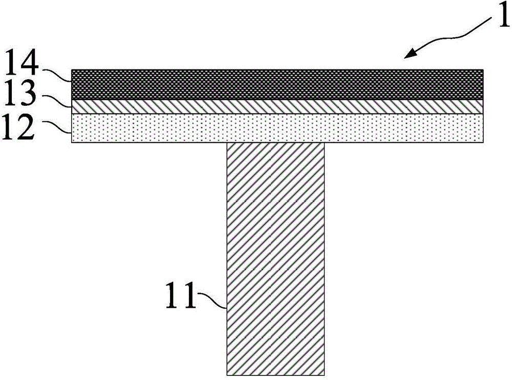
[0044] The invention provides a preparation method of a phase change memory, the phase change memory contains Cr x Sb y Te 1 Phase change material, its preparation process is as follows:
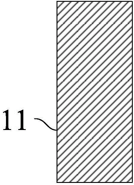
[0045] Step 1: forming the lower electrode layer 11 .
[0046] Such as figure 2 As shown, using sputtering method, evaporation method, chemical vapor deposition (CVD), plasma enhanced chemical vapor deposition (PECVD), low pressure chemical vapor deposition (LPCVD), metal compound vapor deposition (MOCVD), molecular beam The lower electrode layer 11 is prepared by any one of epitaxy (MBE), atomic vapor deposition (AVD) or atomic layer deposition (ALD). In this embodiment, the lower electrode layer is prepared by chemical vapor deposition 11.
[0047] The material of the lower electrode layer 11 is one of the single metal materials W, Pt, Au, Ti, Al, Ag, Cu or Ni, or an alloy material composed of any two or more of the single metal materials , or the nitride or oxide of the single meta...
Embodiment 2
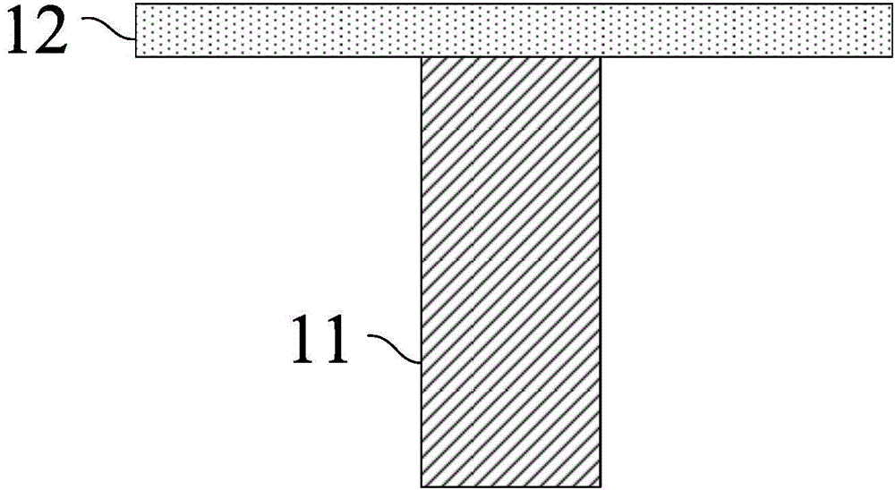
[0059] The present invention provides a method for preparing a phase-change memory. This embodiment adopts the same technical solution as Embodiment 1. The difference is that the method for preparing the phase-change material layer 12 is changed to the atomic vapor deposition method, and the remaining steps are the same as Embodiment 1 is completely the same, and can also achieve the same technical effect.
Embodiment 3
[0061] The present invention provides a method for preparing a phase-change memory. This embodiment adopts the same technical solution as that of Embodiment 1 and Embodiment 2, and the difference is that the Sb in Embodiment 1 and Embodiment 2 2.5 Te 1 Alloy target changed to Sb 2 Te 1 alloy target. The rest of the steps are exactly the same as those in Embodiment 1 and Embodiment 2.
PUM
| Property | Measurement | Unit |
|---|---|---|
| Diameter | aaaaa | aaaaa |
| Height | aaaaa | aaaaa |
| Thickness | aaaaa | aaaaa |
Abstract
Description
Claims
Application Information


