Adiabatic logic circuit and single bit full adder

An adiabatic logic circuit and circuit technology, applied in logic circuits, electrical components, pulse technology and other directions, can solve the problems of the circuit not working properly, the circuit layout and wiring is difficult, and the full swing can not be achieved, so as to avoid the output node dangling, The effect of reducing the number of transistors and reducing power consumption

Active Publication Date: 2015-03-11
SHANDONG LANDBRIDGE PETROCHEMICAL CO LTD
View PDF4 Cites 5 Cited by
  • Summary
  • Abstract
  • Description
  • Claims
  • Application Information

AI Technical Summary

Problems solved by technology

The dual-rail structure of the input signal makes circuit layout and wiring difficult, and the signal transmission structure of dual-rail input and dual-rail output requires symmetrical logic input signals, so the number of transistors is relatively large, which makes the layout and wiring in the design more complicated; some traditional The output node of the adiabatic logic circuit is suspended, so that the output level is easily affected by the noise in the circuit due to the coupling effect of the parasitic capacitance, causing the circuit to fail to work normally; (Efficient Charge Recovery Logic, referred to as ECRL) circuit, causing more energy loss in the circuit

Method used


Image

  • Adiabatic logic circuit and single bit full adder
  • Adiabatic logic circuit and single bit full adder
  • Adiabatic logic circuit and single bit full adder

Examples


Embodiment 1

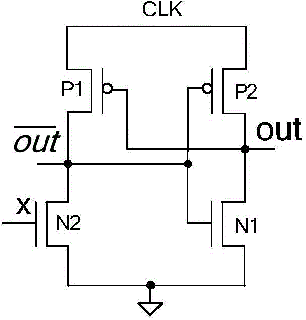
[0021] Example one: such as figure 1 As shown, an adiabatic logic circuit includes a logic evaluation circuit, an energy recovery circuit, and a first NMOS tube N1. The energy recovery circuit is composed of a first PMOS tube P1 and a second PMOS tube P2. The drains of the first PMOS tube P1 are respectively Connected to the substrate of the first PMOS tube P1, the drain of the second PMOS tube P2, the substrate of the second PMOS tube P2 and the external power clock signal terminal CLK, the gate of the first PMOS tube P1 is connected to the second PMOS tube respectively The source of P2 is connected to the drain of the first NMOS transistor N1. The source of the first PMOS transistor P1 is connected to the gate of the second PMOS transistor P2, the energy transmission end of the logic evaluation circuit, and the gate of the first NMOS transistor N1. Connected, the logic evaluation circuit includes a second NMOS transistor N2, the drain of the second NMOS transistor N2 is connec...

Embodiment 2

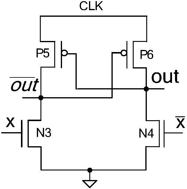
[0027] Embodiment two: such as image 3 As shown, the rest is the same as the first embodiment. The difference is that the logic assignment circuit includes the fifth NMOS tube N5, the sixth NMOS tube N6, the seventh NMOS tube N7, and the eighth NMOS tube N8. The fifth NMOS tube N5 The drain is connected to the source of the first PMOS transistor P1 and the drain of the sixth NMOS transistor N6, the source of the fifth NMOS transistor N5 is connected to the drain of the seventh NMOS transistor N7, and the source of the seventh NMOS transistor N7 They are connected to the source and external ground of the eighth NMOS transistor N8 respectively, and the source of the sixth NMOS transistor N6 is connected to the drain of the eighth NMOS transistor N8. The adiabatic logic circuit formed by the above logic evaluation circuit realizes exclusive OR / identical The logic function of the OR gate, where the gate of the fifth NMOS transistor N5 is the first signal input terminal X, the gate ...

Embodiment 3

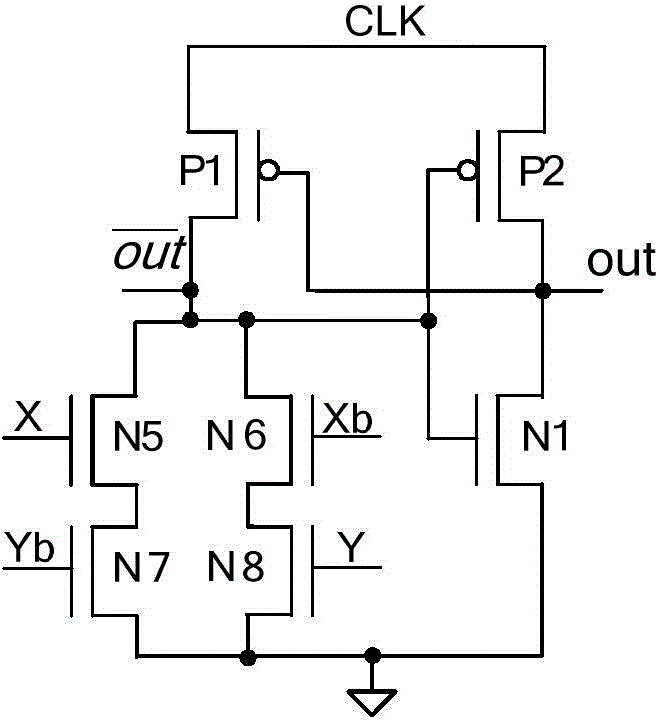
[0028] Example three: such as Figure 4 As shown, the rest is the same as the first embodiment. The difference is that the logic assignment circuit includes a ninth NMOS tube N9, a tenth NMOS tube N10, an eleventh NMOS tube N11, a twelfth NMOS tube N12, and a thirteenth NMOS tube. Tube N13, the drain of the ninth NMOS tube N9 are respectively connected to the drain of the tenth NMOS tube N10, the drain of the eleventh NMOS tube N11, and the source of the first PMOS tube P1, and the source of the ninth NMOS tube N9 Connected to the drain of the twelfth NMOS transistor N12, the gate of the ninth NMOS transistor N9 is connected to the gate of the eleventh NMOS transistor N11, and the source of the twelfth NMOS transistor N12 is respectively connected to the external ground terminal and the thirteenth The source of the NMOS transistor N13 is connected, the source of the tenth NMOS transistor N10 is connected to the source of the eleventh NMOS transistor N11 and the drain of the thir...


PUM


Abstract

The invention discloses an adiabatic logic circuit, which is characterized by comprising a logic assignment circuit, an energy recovery circuit and a first N-channel metal oxide semiconductor (NMOS) transistor, wherein the energy recovery circuit consists of a first P-channel metal oxide semiconductor (PMOS) transistor and a second PMOS transistor. The adiabatic logic circuit has the advantages that a logic signal is only input into single module of the logic assignment circuit, a normal phase output signal is output from the grid of the first PMOS transistor, and an inverse output signal is output from an energy transmission end of the logic assignment circuit; the circuit structure adopts signal transmission manners of one-way input and two-way output, so that circuit design is simplified, the quantity of transistors is reduced, and cascade connection between the circuit and other unit circuits is easier; furthermore, as the energy transmission end of the logic assignment circuit is connected with the grid of the first NMOS transistor and the first NMOS transistor has the function of clamping, an output node is prevented from floating to some extent, the output performance of the circuit is improved, and the power consumption of the whole circuit is effectively reduced finally.

Description

Technical field [0001] The invention relates to an adiabatic circuit structure, in particular to an adiabatic logic circuit and a one-bit full adder. Background technique [0002] Nowadays, the design process of integrated circuit technology has entered the nano stage. In the process of chip design, no matter from the cost and performance of the chip itself, or from the perspective of the market of electronic information products, power consumption has become an important indicator to measure chip performance. Low-power design has become a hot and difficult point in current chip design. [0003] The adiabatic circuit is also called the energy recovery circuit. It has been widely used in the design of large-scale integrated circuits in the recent period and is a new type of low-power circuit design technology. Its basic principle is to use an AC power supply to supply power to it. By recovering the charge of the node capacitance, the energy in the circuit is reused many times to ac...

Claims


Application Information

Patent Timeline
Patent Type & Authority Applications(China)
IPC IPC(8): H03K19/094
Inventor 胡建平耿烨亮
Owner SHANDONG LANDBRIDGE PETROCHEMICAL CO LTD
Why Eureka
Try Eureka