Three dimension (3D) printing method for multilayer flexible circuit board
A flexible circuit board and 3D printing technology, which is applied in multilayer circuit manufacturing, printed circuit, printed circuit manufacturing, etc., can solve problems such as the production disadvantages of multilayer flexible circuit boards, and achieve low production costs, high precision, and simple processes. Effect
- Summary
- Abstract
- Description
- Claims
- Application Information
AI Technical Summary
Problems solved by technology
Method used
Image

Examples
Embodiment Construction
[0015] In order to make the above-mentioned features and advantages of the present invention more comprehensible, the following specific embodiments are described in detail in conjunction with the accompanying drawings.
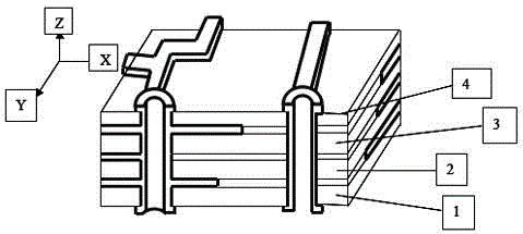
[0016] The invention relates to a 3D printing method of a multilayer flexible circuit board, which is carried out according to the following steps:
[0017] 1) Provide the substrate material, which is composed of polyimide powder, polyester powder and acrylic UV shadowless glue; the materials provided as the metal conductor part are copper powder, cobalt-chromium alloy powder, gold powder and silver powder. ;
[0018] 2) Printing starts from the bottom circuit board of the multi-layer flexible circuit board, and prints each layer obtained by cutting layer by layer according to the 3D CAD model in a specific direction. The printing direction of each layer is first the x-axis direction and then the y-axis direction , the printing starting point is the vertex i...
PUM
| Property | Measurement | Unit |
|---|---|---|
| Thickness | aaaaa | aaaaa |
Abstract
Description
Claims
Application Information
PatSnap Eureka turns technology decisions into work you can execute. Powered by our Innovation Knowledge Graph, it runs expert workflows across engineering, life sciences, materials and intellectual property. Get your review-ready output in minutes.


