Confirmation method for alignment achieved in wafer test

A wafer test and wafer technology, applied in the field of confirmation of position alignment in wafer test, can solve the problems of wasting wafer test time, affecting product quality, and wrong relationship between wafer map positions, so as to avoid position Alignment deviation, prevention of positional alignment errors, and the effect of saving test time

Active Publication Date: 2017-10-24
SHANGHAI HUAHONG GRACE SEMICON MFG CORP
View PDF13 Cites 0 Cited by
  • Summary
  • Abstract
  • Description
  • Claims
  • Application Information

AI Technical Summary

Problems solved by technology

[0003] As we all know, the camera system of the probe station has the minimum resolution. When the feature chip is too small, or the relevant parameter settings are abnormal, or when there is chromatic aberration in the manufacturing process of the wafer, the probe station’s accuracy of the initial position of the wafer There will be deviations in the identification, which will lead to errors in the corresponding relationship between the wafer map and the actual wafer, resulting in a positional offset in the wafer map (such as image 3 shown)
If this situation is not discovered in time during wafer-level testing, it will lead to errors in the normal picking of chips in subsequent packaging tests. In serious cases, abnormal chips will be picked as good chips, which will seriously affect product quality.
In particular, chips at this stage are becoming more and more complex. There are more than 20,000 chips on a wafer, and there are often more than two testing procedures, such as high-temperature testing, normal temperature testing, low-temperature testing, specific project testing, and testing in a certain process. When an abnormality is found in the
If in a process test, the position of the wafer is identified incorrectly, it will seriously waste the wafer test time and affect the test quality of the chip

Method used


Image

  • Confirmation method for alignment achieved in wafer test
  • Confirmation method for alignment achieved in wafer test
  • Confirmation method for alignment achieved in wafer test

Examples


Embodiment Construction

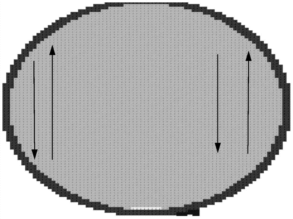
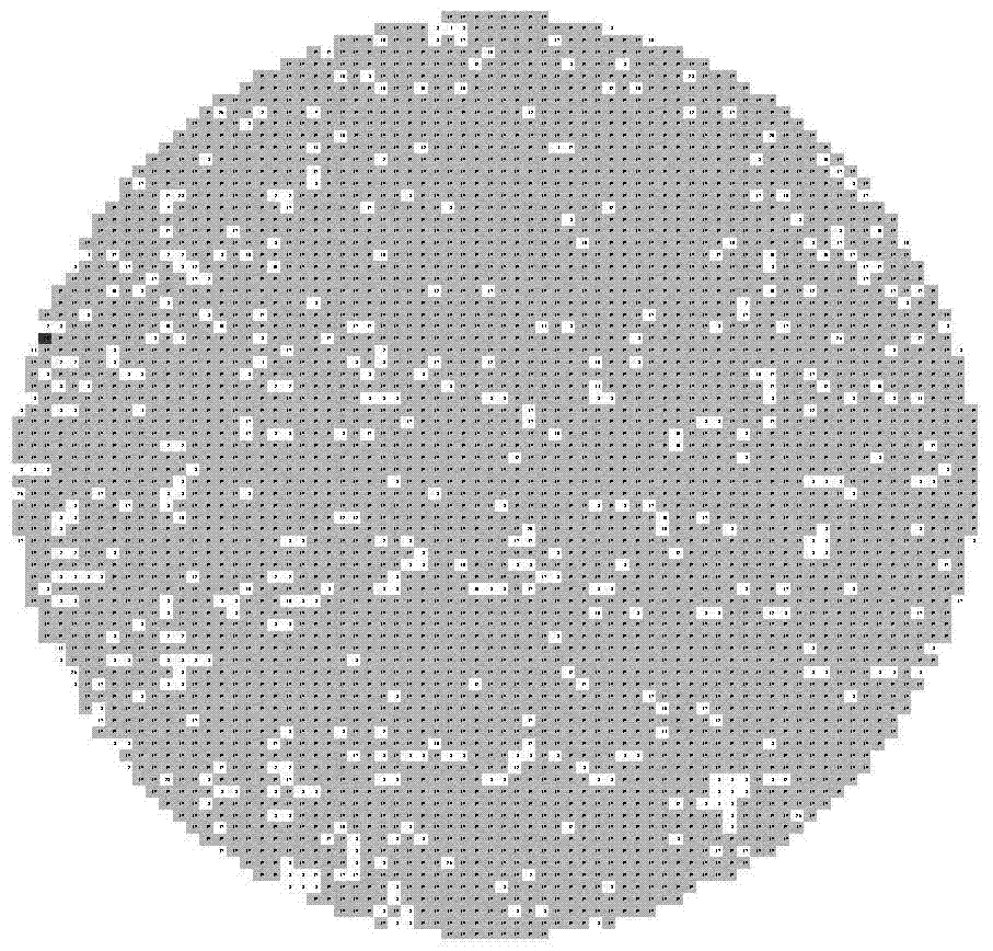
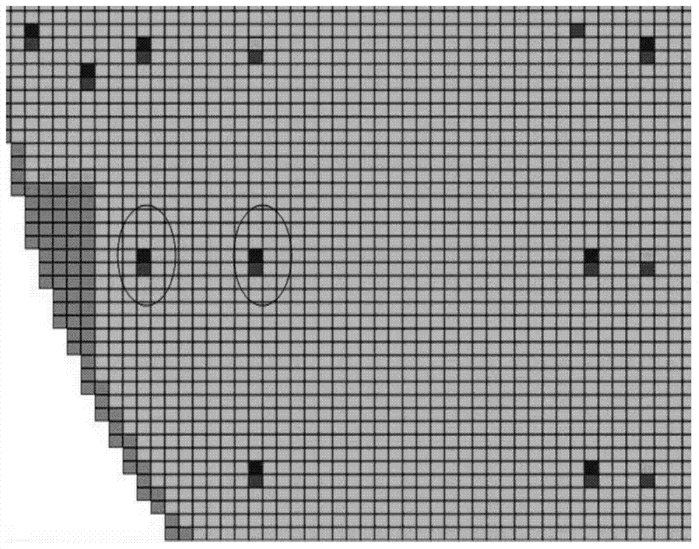
[0019] The method for confirming position alignment in the wafer test of the present invention is to carry out more than two positions of the test process on a wafer containing a chip of NVM IP (non-volatile memory intellectual property, non-volatile memory Intellectual Property) Alignment confirmation method, the steps comprising:

[0020] 1) The address Z of the memory area of ​​the chip is first specified as the location of the memory mapping address, and the address Z contains at least one byte; the chip also contains a flag bit of the chip state, and the flag bit can be composed of one byte;

[0021] If the chip with address Z area is normal, information such as 0X5A can be written in the flag bit. Confirm that there is at least one target chip Tai according to the required position, where "i" can be 1, 2, 3 or more. If there is one hour, record it as Ta1; if there are two hours, record it as Ta1, Ta2; and so on.

[0022] In order to improve the test efficiency, the sel...


PUM


Abstract

The invention discloses a method for confirming position alignment in a wafer test, comprising: 1) first specifying that the address Z of the memory area of ​​the chip is the position for storing the mapping address, and the chip also includes a flag bit of the chip state; 2) In the first test process, the tester reads the chip position A information on the wafer from the probe station system, and writes the corresponding mapping relationship into the corresponding chip on the wafer through the tester; 3) In the second and subsequent process tests, compare the chip position A read by the probe station system with the position A' read from the target chip. If they are not the same, the tester will alarm; if they are consistent, continue follow-up tests. The invention avoids the situation that position alignment shifts in the multi-process test, saves the test time of the wafer, and guarantees the test quality of the wafer to the greatest extent.

Description

technical field [0001] The invention relates to a position alignment method in the field of semiconductor testing, in particular to a method for confirming position alignment in wafer testing. Background technique [0002] In existing semiconductor testing at the wafer level, the testing of wafer chips relies on a prober system for position alignment and confirmation. During the test, when the wafer is transferred to the chuck of the probe station, the probe station system uses its internal camera system to identify and confirm the initial position of the characteristic chip on the wafer. After the initial position is obtained, the test Among them, the probe station is set according to the expected wafer map (map) (such as figure 1 shown) to perform the needle stick test, or perform the needle stick test in the wafer map (map) according to the moving position sent by the tester. After the test is completed, a wafer map (map) of test results will be obtained (such as figu...

Claims


Application Information

Patent Timeline
Patent Type & Authority Patents(China)
IPC IPC(8): G01R31/26
Inventor 谢晋春辛吉升
Owner SHANGHAI HUAHONG GRACE SEMICON MFG CORP
Why Eureka
Try Eureka