Manufacturing method for low-temperature polycrystalline silicon and manufacturing method for TFT substrate

A technology of low-temperature polysilicon and its production method, which is applied in the manufacture of semiconductor/solid-state devices, semiconductor devices, electrical components, etc. It can solve the problems of polysilicon layer with many metal residues, expensive ELA equipment, and low density of polysilicon gap states, so as to reduce crystallization Process temperature, shorten crystallization process time, and improve crystallization effect

Active Publication Date: 2015-03-25
TCL CHINA STAR OPTOELECTRONICS TECH CO LTD
View PDF13 Cites 6 Cited by
  • Summary
  • Abstract
  • Description
  • Claims
  • Application Information

AI Technical Summary

Problems solved by technology

[0005] The polysilicon grain size obtained by the CVD crystallization process is extremely small, and the deposition rate is low; the traditional SPC crystallization process requires high temperature and takes a long time, resulting in easy deformation of the substrate and high cost; the polysilicon layer metal produced by the MIC or MILC crystallization process There are many residues, which lead to the deterioration of TFT electrical properties; polysilicon produced by ELA crystallization process has a low gap state density, it is difficult to prepare large-area polysilicon thin films, and ELA equipment is expensive

Method used


Image

  • Manufacturing method for low-temperature polycrystalline silicon and manufacturing method for TFT substrate
  • Manufacturing method for low-temperature polycrystalline silicon and manufacturing method for TFT substrate
  • Manufacturing method for low-temperature polycrystalline silicon and manufacturing method for TFT substrate

Examples


Embodiment Construction

[0052] In order to further illustrate the technical means adopted by the present invention and its effects, the following describes in detail in conjunction with preferred embodiments of the present invention and accompanying drawings.

[0053] see Figure 6 and Figure 8 to Figure 13 , the invention provides a method for manufacturing low-temperature polysilicon, comprising the steps of:

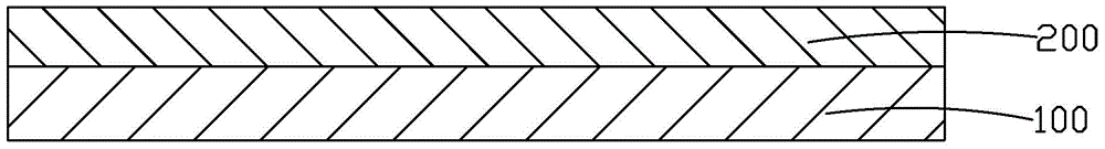
[0054] Step 1, providing a substrate 1 .

[0055] The substrate 1 is a common transparent substrate, preferably, the substrate 1 is a glass substrate.

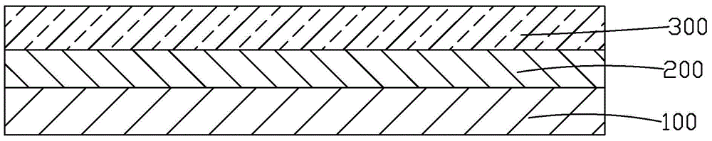
[0056] Step 2, such as Figure 8 As shown, a buffer layer 2 is deposited on a substrate 1 .

[0057] Specifically, the buffer layer 2 may be a single layer of SiNx, a single layer of SiOx, a double layer of SiNx, a double layer of SiOx, or a combination of both SiNx and SiOx layers.

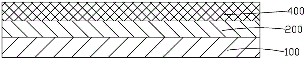
[0058] Step 3, if Figure 9 As shown, a metal mesh film 3 is coated on the buffer layer 2.

[0059] Specifically, the metal mesh 3 is made of aluminum. ...


PUM


Abstract

The invention provides a manufacturing method for low-temperature polycrystalline silicon and a manufacturing method for a TFT substrate. The manufacturing method for the low-temperature polycrystalline silicon includes the following steps that S1, a substrate (1) is provided; S2, a buffering layer (2) is deposited on the substrate (1); S3, a metal mesh film (3) is plated on the buffering layer (2); S4, an amorphous silicon layer (4) is deposited on the metal mesh film (3); S5, rapid thermal annealing is carried out on the amorphous silicon layer (4), and therefore the amorphous silicon layer (4) is crystallized and converted into a polycrystalline silicon layer (5); S6, the metal mesh film (3) is removed. The method can effectively reduce the temperature of the crystallization manufacture procedure, shorten the time for the crystallization manufacture procedure, reduce the cost for preparing polycrystalline silicon thin films in a large-area mode, improve the crystallization effect and make crystalline grains larger and more uniform.

Description

technical field [0001] The invention relates to the field of display technology, in particular to a method for manufacturing low-temperature polysilicon and a method for manufacturing a TFT substrate using the method. Background technique [0002] With the development of flat panel displays, the demand for panels with high resolution and low energy consumption is constantly being raised. Due to its high electron mobility, Low Temperature Poly-Silicon (LTPS) has attracted the attention of the industry in the technology of Liquid Crystal Display (LCD) and Organic Light Emitting Diode (OLED) , is regarded as an important material to realize low-cost full-color flat panel display. For flat-panel displays, the use of low-temperature polysilicon materials has the advantages of high resolution, fast response, high brightness, high aperture ratio, and low energy consumption, and low-temperature polysilicon can be produced at low temperatures and can be used to make C-MOS circuits. ...

Claims


Application Information

Patent Timeline
Patent Type & Authority Applications(China)
IPC IPC(8): H01L21/02H01L21/336
CPCH01L21/02532H01L21/02595H01L21/02667H01L27/1274H01L27/1277H01L27/1285H01L21/02422H01L21/02488H01L21/02491H01L21/02502H01L21/02672H01L27/1262H01L29/66757H01L27/1218H01L27/1222H01L21/02164H01L21/0217H01L21/02425H01L21/02592H01L21/30604H01L21/324
Inventor 李亚
Owner TCL CHINA STAR OPTOELECTRONICS TECH CO LTD
Why Eureka
Try Eureka