MoS2/Si p-n junction solar cell device and preparation method thereof

A solar cell and device technology, applied in electrical components, semiconductor devices, circuits, etc., can solve the problems of light absorption and electron transfer defects, complex preparation process, high rate of defective products, etc., achieve weak light-induced attenuation effect, repeatable High performance and fast response time

Inactive Publication Date: 2015-03-25
CHINA UNIV OF PETROLEUM (EAST CHINA)
View PDF2 Cites 16 Cited by
  • Summary
  • Abstract
  • Description
  • Claims
  • Application Information

AI Technical Summary

Problems solved by technology

However, single-layer MoS 2 Defects in both light absorption and electron transfer
Shanmugam et al. proposed multilayer MoS deposited on ITO glass 2 Form a Schottky junction with metal gold (Au), and the

Method used


Image

  • MoS2/Si p-n junction solar cell device and preparation method thereof
  • MoS2/Si p-n junction solar cell device and preparation method thereof
  • MoS2/Si p-n junction solar cell device and preparation method thereof

Examples


Example Embodiment

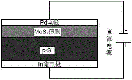
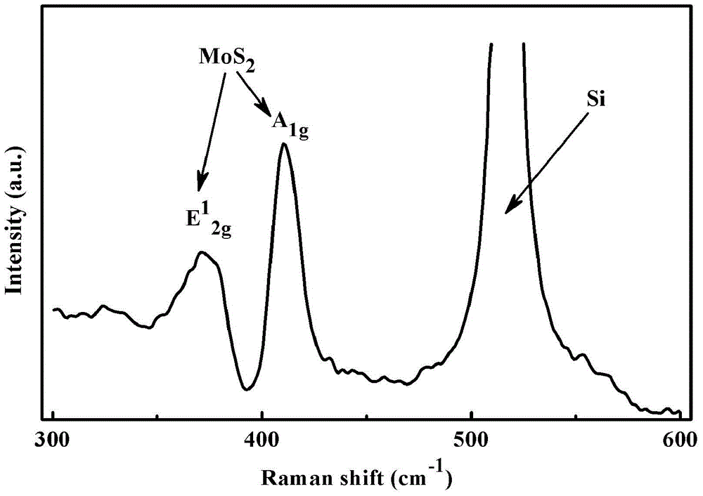
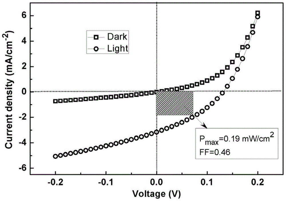
[0029] The present invention utilizes DC magnetron sputtering technology to deposit MoS on p-Si semiconductor substrate 2 Thin film layer, forming a p-n junction. When there is light, under the action of the built-in electric field, the photogenerated carriers diffuse and drift, and finally a stable photogenerated voltage is formed at both ends of the p-n junction, that is, the photovoltaic effect.

[0030] Next to MoS 2 / Si p-n junction solar cell device structure and preparation methods are described in detail.

[0031] A kind of MoS 2 / Si p-n junction solar cell devices, including MoS 2 Thin film layer, as MoS 2 The Si substrate of the thin film layer carrier, the metal Pd front electrode and the metal In back electrode. MoS 2 The thin film layer is set on the surface of Si substrate, MoS 2 The thickness of the film layer is 70-80nm, the Si substrate is a p-type Si single crystal substrate, and the resistivity is 1.2-1.8Ω·cm. Metal Pd front electrode set on MoS 2 On...


PUM

PropertyMeasurementUnit
Thicknessaaaaaaaaaa
Thicknessaaaaaaaaaa
Thicknessaaaaaaaaaa

Abstract

The invention discloses a MoS2/Si p-n junction solar cell device and a preparation method of the MoS2/Si p-n junction solar cell device. The MoS2/Si p-n junction solar cell device comprises a MoS2/Si thin film layer, a Si substrate serving as a thin film layer carrier, a metal Pd front electrode and a metal In back electrode. The n-type MoS2 thin film is deposited on the surface of the p-type Si substrate, a p-n junction is formed, and the MoS2/Si p-n junction solar cell device is developed. The method comprises the steps of preparation of the MoS2/Si p-n junction and preparation of metal electrodes, wherein firstly the magnetron sputtering technology is adopted, the MoS2 thin film is deposited on the surface of the p-type Si substrate, then preparation of the metal Pd front electrode and the metal In back electrode is finished, and the integral cell device is formed. The performance testing result shows that the MoS2/Si p-n junction solar cell device has the obvious photovoltaic characteristic, and under the lighting condition of 15 mW/cm<2>, the short circuit current is 3.16 mA/cm<2>, the open circuit voltage is 0.13 V, the fill factor is 0.46 and the conversion efficiency is 1.3%.

Description

technical field [0001] The invention belongs to the field of new energy solar photovoltaics, and in particular relates to a MoS 2 / Si p-n junction solar cell device, and preparation of MoS based on magnetron sputtering technology 2 / Si p-n junction solar cell device method. Background technique [0002] Since the beginning of the 21st century, with the development of society and the improvement of people's living standards, people's demand for energy has increased dramatically. The depletion of traditional fossil energy and the damage to the environment are gradually emerging, forcing countries to take the development and utilization of new energy as a national future energy development strategy. Solar energy is the most common among new energy sources, and it has been used by people earlier, and it has the advantages of good compatibility with electric power technology and high safety. A solar cell is a common device that converts solar energy into electricity. At prese...

Claims


Application Information

Patent Timeline
IPC IPC(8): H01L31/072H01L31/18
CPCH01L31/074H01L31/18Y02E10/50Y02P70/50
Inventor 郝兰众高伟刘云杰韩治德薛庆忠
Owner CHINA UNIV OF PETROLEUM (EAST CHINA)
Why Eureka
Try Eureka