LED (light-emitting diode) chip cutting cutter with novel structure and LED chip cutting method

A technology of LED chips and cutting tools, which is applied in the direction of manufacturing tools, fine working devices, electrical components, etc., can solve the problems of high cost, easily damaged crystal grains, multiple cutting, etc., achieve small amplitude, increase stability, The effect of simple loading and unloading process

Active Publication Date: 2015-04-01
马鞍山太时芯光科技有限公司
View PDF9 Cites 9 Cited by
  • Summary
  • Abstract
  • Description
  • Claims
  • Application Information

AI Technical Summary

Problems solved by technology

[0006] Aiming at the problems existing in the existing chip cutting technology, such as high cost, multiple cuts, and easily da

Method used


Image

  • LED (light-emitting diode) chip cutting cutter with novel structure and LED chip cutting method
  • LED (light-emitting diode) chip cutting cutter with novel structure and LED chip cutting method
  • LED (light-emitting diode) chip cutting cutter with novel structure and LED chip cutting method

Examples


Embodiment 1

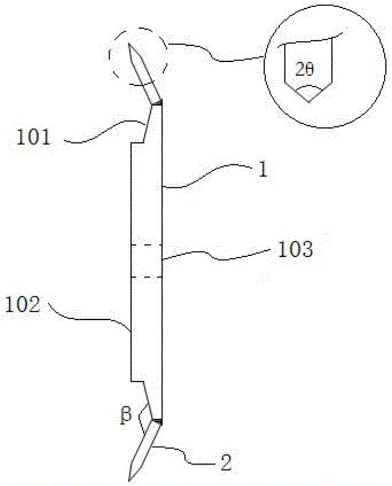
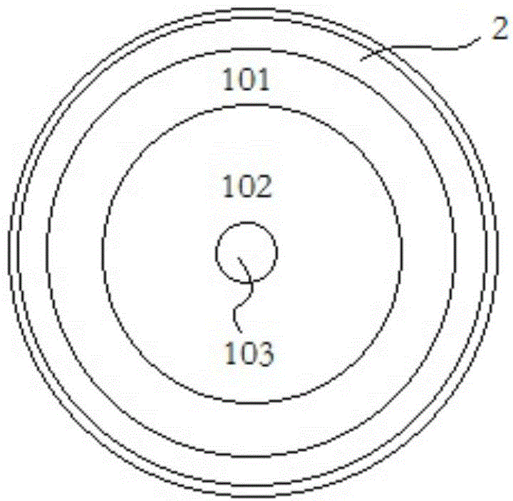
[0040] Such as figure 1 and figure 2 As shown, a LED chip cutting tool with a new structure includes a flange 1 and a blade 2. The flange 1 is disc-shaped, made of aluminum alloy, and has a flange protrusion 101 in the middle, and its thickness is uniform. The edge is provided with a flange transition 102, the thickness of which gradually decreases towards the outer edge, and the middle part of the flange protrusion 101 is provided with a mounting hole 103 with a diameter of 19mm; the blade 2 is circular and fixed on the outer edge of the flange transition 102, The angle between the blade 2 and the flange 1 is β=135°, the blade width of the blade 2 is 21 μm, and the slope θ of the blade is 20°. The diameter is 0.1-2.5 μm.

[0041] A method for cutting an LED chip, the steps of which are: using a special knife changing tool for a DISCO cutting machine to change the above-mentioned cutting knife to a cutting machine, and use a special whetstone to sharpen the knife after the ...

Embodiment 2

[0044] A LED chip cutting tool with a new structure, the structure is the same as that of Embodiment 1, the difference is that the angle between the blade 2 and the flange 1 is β=140°, the blade width of the blade 2 is 25 μm, and the slope θ of the blade is 22°. The cutting edge of the blade 2 is formed by the organic combination of diamond abrasive grains and a binder, and the diameter of the diamond abrasive grains is 2.5-5 μm.

[0045] A LED chip cutting method, the steps are the same as in Example 1, the difference is: when cutting the chip in half, the cutting height is set to 0.180mm, the cutting knife speed is set to 40mm / s; the baking temperature is 80°C, and the baking time 20 minutes; when cutting through the chip, the cutting height is set to 0.080mm, and the cutting knife speed is set to 10mm / s.

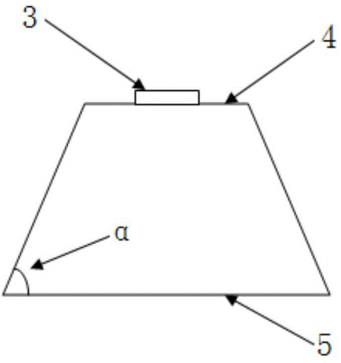
[0046] The angle between the slope of the chip cut in this embodiment and the N surface is 40°. The chip with this structure can shorten the path of light propagating ins...

Embodiment 3

[0048] A LED chip cutting tool with a new structure, the structure is the same as that of Embodiment 1, the difference is: the angle β between the blade 2 and the flange 1=145°, the blade width of the blade 2 is 23 μm, and the slope θ of the blade is 25°, The cutting edge of the blade 2 is formed by the organic combination of diamond abrasive grains and a binder, and the diameter of the diamond abrasive grains is 5-8 μm.

[0049] A LED chip cutting method, the steps are the same as in Example 1, the difference is: when cutting the chip in half, the cutting height is set to 0.250mm, the cutting knife speed is set to 30mm / s; the baking temperature is 100°C, and the baking time 10 minutes; when cutting through the chip, the cutting height is set to 0.070mm, and the cutting speed is set to 40mm / s.

[0050] The included angle between the slope of the chip cut in this embodiment and the N surface is 35°. The chip with this structure can shorten the path of light propagating inside t...


PUM

PropertyMeasurementUnit
Diameteraaaaaaaaaa

Abstract

The invention discloses an LED (light-emitting diode) chip cutting cutter with a novel structure and an LED chip cutting method, which belong to the field of semiconductor device processing. The LED chip cutting cutter comprises a flange plate and a blade, wherein the flange plate is shaped like a disk, the center of the flange plate is provided with a flange bulge, the edge is provided with a flange transition, and the center of the flange bulge is provided with a mounting hole; the blade is shaped like a ring, and is fixed at the outer edge of the flange transition. The LED chip cutting cutter is highly stable under the condition of high-speed rotation, and is convenient to mount and dismount. By taking the cutting cutter as a cutting tool, the cutting method can be adopted to directly cut out chips with a trapeziform structure, cutting time is shortened, cutting efficiency is increased, and the cut chips are not damaged, and are high in luminous efficiency.

Description

technical field [0001] The invention belongs to the field of semiconductor device processing, and more specifically relates to a cutting tool for cutting LED chips with a novel structure and a cutting method for cutting LED chips. Background technique [0002] During the manufacturing process of semiconductor chips, crystal grains are generally arranged in a rectangular shape on the surface of the chip, and the surface of the chip is provided with grid-shaped dicing lines along the periphery of the crystal grains to separate each crystal grain. Existing chip cutting methods mainly include cutter (such as diamond cutter) cutting and radiant energy (such as laser) cutting. Knife cutting is to use mechanical force to directly act on the dicing road of the chip to realize the separation of crystal grains. Laser cutting is a non-contact cutting method, which obtains high energy density after laser energy is optically focused, and directly vaporizes the chip along the cutting lin...

Claims


Application Information

Patent Timeline
IPC IPC(8): B28D5/00H01L33/00
CPCB28D5/0058B28D5/022H01L33/00
Inventor 董成靖明亮廖伟李有群廉鹏
Owner 马鞍山太时芯光科技有限公司
Why Eureka
Try Eureka