Large-area online measurement device and method for geometrical parameters of nano-structure

A technology of nanostructure and geometric parameters, applied in the direction of measuring devices, optical devices, instruments, etc., can solve problems affecting the efficiency of sample analysis and testing, meet the requirements of non-contact and non-destructive measurement, broad application prospects, and promote the expansion of applications Effect

Inactive Publication Date: 2015-04-01
HUAZHONG UNIV OF SCI & TECH
View PDF10 Cites 21 Cited by
  • Summary
  • Abstract
  • Description
  • Claims
  • Application Information

AI Technical Summary

Problems solved by technology

At the same time, the above-mentioned optical scattering measurement technology can only perform single-point testing. If you want to obtain the distribution information of the parameters to be measured at multiple points on the sample or in a large area, you need to move the sample stage for multiple tests or point-to-point scanning, which will seriously affect the quality of the sample. Analyzing Test Efficiency

Method used


Image

  • Large-area online measurement device and method for geometrical parameters of nano-structure
  • Large-area online measurement device and method for geometrical parameters of nano-structure
  • Large-area online measurement device and method for geometrical parameters of nano-structure

Examples


example

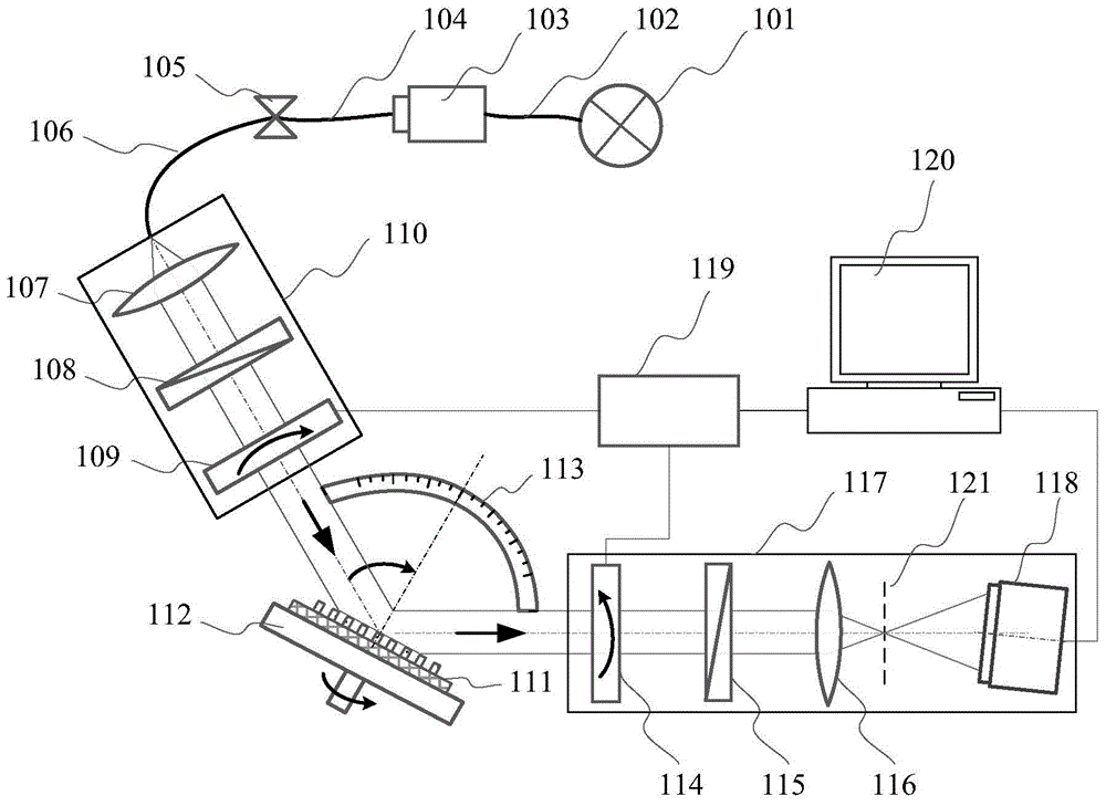
[0054] In the first step, the nanostructure 111 to be tested is placed on the rotating sample stage 112;

[0055] In the second step, the light emitted by the xenon lamp light source is turned into monochromatic light by the monochromator, and the monochromatic light is introduced into one end of the polarizer arm 110 through the fiber coupler 105 and the outgoing fiber 106, and then becomes parallel through the collimating mirror 107 The light beam is polarized by the polarizer 108, and the phase compensator 109 at the end of the polarizer arm is phase-modulated and projected onto the surface of the nanostructure 111 to be tested;

[0056] In the third step, after the parallel light beam is reflected from the surface of the nanostructure 111 to be tested, it is phase-modulated by the phase compensator 114 at the end of the analyzer arm, and analyzed by the analyzer 115, and enters the area array detector 118 through the imaging lens 116. The image collected by the CCD detecto...


PUM


Abstract

The invention discloses a large-area online measurement device and a large-area online measurement method for geometrical parameters of a nano-structure. The three-dimensional microscopic morphology of the nano-structure in a large-area region containing an entire viewing field can be obtained. Light emitting from a light source is changed into monochromatic light through a monochromator, the monochromatic light sequentially passes through a collimating mirror, a polarizer and a polarizing arm-end phase compensator to obtain an elliptical polarized beam, and then the elliptical polarized beam is projected to the surface of the to-be-measured nano-structure; a light intensity signal corresponding to zero-stage diffraction light in a reflected beam of the to-be-measured nano-structure is acquired, and a measurement imaging Muller matrix of the to-be-measured nano-structure is calculated; geometrical parameter values of the to-be-measured nano-structure at corresponding pixel points are obtained by matching extraction, and the geometrical parameter extraction values at all the pixel points form the three-dimensional microscopic morphology of the to-be-measured nano-structure. A large-area, quick, low-cost, contactless, non-destructive and accurate measurement way can be provided for one-dimensional and two-dimensional sub-wavelength periodic nano-structures involved in a pattern-transfer-based batch manufacturing method such as a photoetching process, a nano-impressing process and other processes.

Description

technical field [0001] The invention belongs to nano-manufacturing, especially the field of on-line process monitoring and optimization control in large-scale nano-manufacturing, and specifically relates to a large-area online measuring device and method for measuring nano-structure geometric parameters such as characteristic line width. , line height, side wall angle, period spacing, overlay error, and large-area online measurement of line edge roughness and line width roughness. Background technique [0002] Nano-manufacturing refers to the manufacturing technology in which the characteristic size of the product is on the order of nanometers, that is, the manufacturing technology in which the characteristic size is within 100nm. In order to achieve effective process monitoring, rapid, low-cost, non-destructive and accurate measurement of the characteristic line width (ie critical dimension), line height, side wall angle and other geometric parameters of nanostructures in n...

Claims


Application Information

Patent Timeline
IPC IPC(8): G01B11/24
Inventor 刘世元陈修国杜卫超张传维
Owner HUAZHONG UNIV OF SCI & TECH
Why Eureka
Try Eureka