Device and method thereof for testing bias temperature instability degrading of MOS (metal oxide semiconductor) device

A MOS device, bias temperature technology, applied in the direction of single semiconductor device testing, etc., can solve the problems of circuit power consumption and chip area increase, and achieve the effect of high test accuracy and simple circuit structure

Active Publication Date: 2015-04-01
EAST CHINA NORMAL UNIVERSITY +1
View PDF10 Cites 16 Cited by
  • Summary
  • Abstract
  • Description
  • Claims
  • Application Information

AI Technical Summary

Problems solved by technology

However, a larger design tolerance will inevitably lead

Method used


Image

  • Device and method thereof for testing bias temperature instability degrading of MOS (metal oxide semiconductor) device
  • Device and method thereof for testing bias temperature instability degrading of MOS (metal oxide semiconductor) device
  • Device and method thereof for testing bias temperature instability degrading of MOS (metal oxide semiconductor) device

Examples


Embodiment Construction

[0023] The present invention will be further described in detail in conjunction with the following specific embodiments and accompanying drawings. The process, conditions, experimental methods, etc. for implementing the present invention, except for the content specifically mentioned below, are common knowledge and common knowledge in this field, and the present invention has no special limitation content.

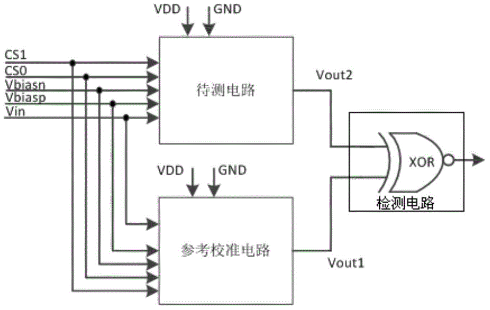
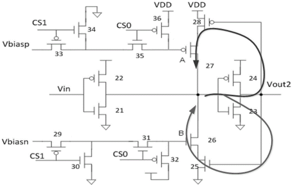
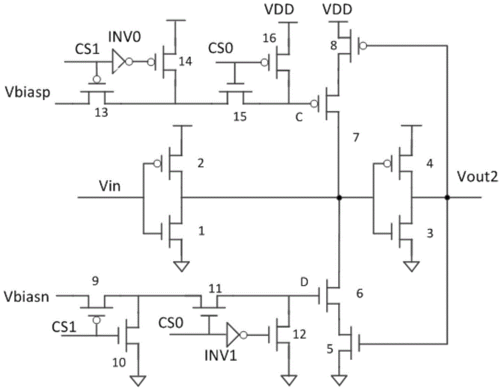
[0024] refer to figure 1 The test device for the degradation of MOS device bias temperature instability of the present invention comprises a circuit to be tested, a reference calibration circuit and a detection circuit; the outputs of the circuit to be tested and the reference calibration circuit are connected to the detection circuit at the same time; the internal setting of the circuit to be tested is the first The feedback control component is connected to the first Schmitt trigger, the first feedback control component is connected to the first Schmitt trigger, and the ...


PUM


Abstract

The invention discloses a device for testing bias temperature instability degrading of a MOS (metal oxide semiconductor) device. The device comprises a to-be-tested circuit, a reference calibration circuit and a detection circuit, wherein the output ends of the to-be-tested circuit and the reference calibration circuit are simultaneously connected with the detection circuit, a first feedback control assembly and a first Schmitt trigger are arranged in the to-be-tested circuit, the first feedback control assembly is used for applying stress on to-be-tested feedback loop components in the first Schmitt trigger so as to generate degrading, the to-be-tested circuit is used for outputting degraded actual hysteresis voltage signals, the reference calibration circuit is used for outputting standard hysteresis voltage signals, and the detection circuit is used for comparing and measuring the difference between the actual hysteresis voltage signals and the reference standard hysteresis voltage signals, so as to test the degrading degree of the feedback loop components. The device has the characteristics that the NBTI (negative bias temperature instability) and PBTI (positive bias temperature instability) properties can be tested, the circuit structure is simple, and the testing accuracy is high. The invention discloses a method for testing the bias temperature instability degrading of the MOS device.

Description

technical field [0001] The invention belongs to the technical field of reliability of semiconductor devices, in particular to a test device for the degradation of bias temperature instability of MOS devices. Background technique [0002] As semiconductor process technology enters the deep submicron era, negative bias temperature instability (NBTI) has become one of the main factors affecting device performance degradation and lifetime. The NBTI effect refers to the degradation of a series of electrical parameters caused by applying a negative gate voltage to a PMOS device at high temperature. The impact on the device is as follows: with the increase of time, the threshold voltage of the PMOS device increases and the leakage current becomes smaller. The limit shrinks, and even the product fails. [0003] Therefore, this makes circuit designers have to consider the impact of NBTI degradation on circuit performance at the product design stage, leaving enough design tolerance ...

Claims


Application Information

Patent Timeline
IPC IPC(8): G01R31/26
Inventor 李小进王艳玲卿健石艳玲胡少坚
Owner EAST CHINA NORMAL UNIVERSITY
Why Eureka
Try Eureka