Preparation methods of controllable arrayed nanowires and FET (field effect transistor) comprising controllable arrayed nanowires

A nanowire and array technology, which is applied in the field of field effect transistor preparation, can solve the problems of poor controllability, difficulty in obtaining large-area array nanowires, and difficulty in realizing controllable array nanowires, and achieves low cost and controllability. Strong, simple craftsmanship

Active Publication Date: 2015-04-01
PEKING UNIV
View PDF5 Cites 2 Cited by
  • Summary
  • Abstract
  • Description
  • Claims
  • Application Information

AI Technical Summary

Problems solved by technology

However, the former is difficult to obtain large-area arrayed nanowires, and the latter ...

Method used


Image

  • Preparation methods of controllable arrayed nanowires and FET (field effect transistor) comprising controllable arrayed nanowires
  • Preparation methods of controllable arrayed nanowires and FET (field effect transistor) comprising controllable arrayed nanowires
  • Preparation methods of controllable arrayed nanowires and FET (field effect transistor) comprising controllable arrayed nanowires

Examples


Embodiment 1

[0045] In this embodiment, the GaN controllable array nanowires are prepared, and the substrate adopts GaN; the pattern of the patterned substrate is a periodic columnar two-dimensional lattice; the growth material of the array nanowires is GaN; the growth method of the array nanowires adopts Molecular beam epitaxy MBE in The growth process is carried out in an ultra-high vacuum growth chamber, and the high-purity (7N) metal source is generated by a K-Cell source furnace; the nitrogen source uses a radio frequency plasma nitrogen source; the growth process uses a reflective High-energy electron diffractometer RHEED in-situ monitoring.

[0046] The preparation method of the controllable array nanowires of this embodiment includes the following steps:

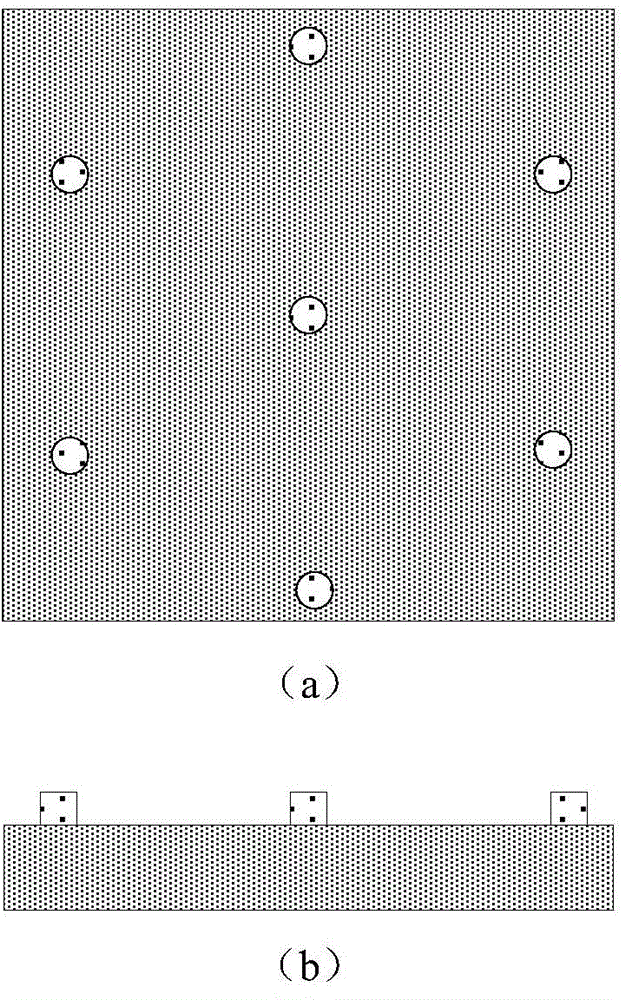
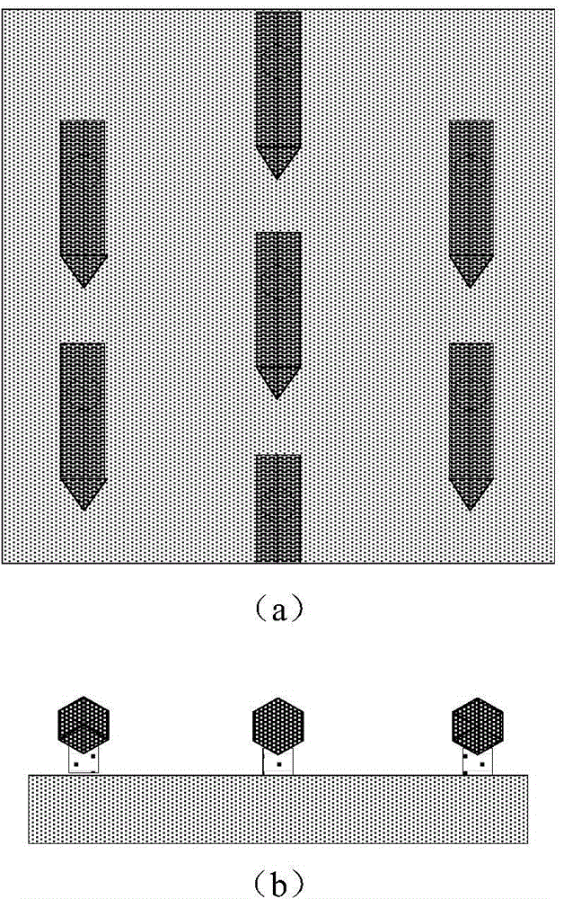
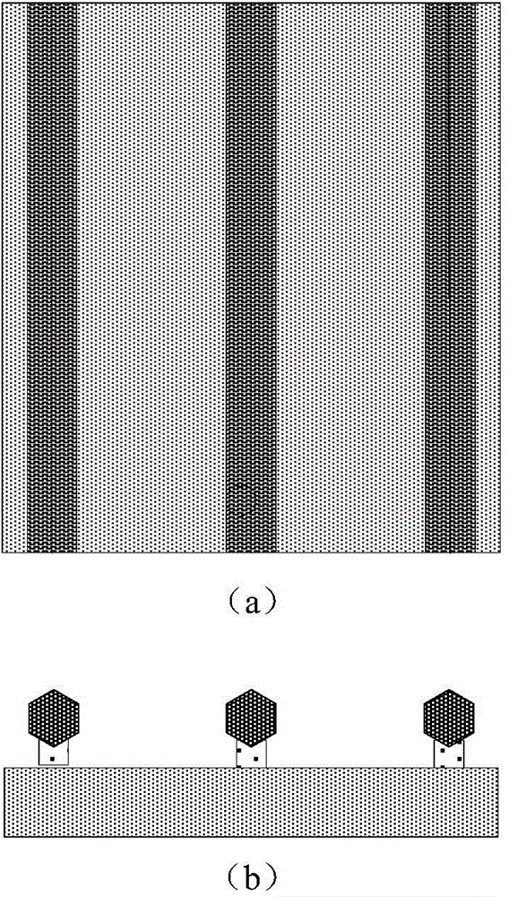
[0047] 1) Select the growth material with anisotropic growth rate along different crystal directions as the substrate:

[0048] The growth rate of wurtzite GaN along the [0001] direction is much faster than that along the an...

Embodiment 2

[0060] In this embodiment, a GaN controllable array nanowire FET is prepared, and the substrate is GaN; the pattern of the patterned substrate is a periodic hole-like two-dimensional lattice; the growth material of the array nanowire is GaN; the growth of the array nanowire The method uses molecular beam epitaxy (MBE) in The growth process is carried out in an ultra-high vacuum chamber, and the high-purity (7N) metal source is generated by a K-Cell source furnace; the nitrogen source is a radio frequency plasma nitrogen source; the growth process uses a reflection RHEED in situ monitoring.

[0061] The preparation method of the controllable array nanowire FET of this embodiment includes the following steps:

[0062] 1) Select the growth material with anisotropic growth rate along different crystal directions as the substrate:

[0063] The growth rate of wurtzite GaN along the [0001] direction is much faster than that along the and The growth rate in the direction, choos...


PUM


Abstract

The invention discloses a preparation method of controllable arrayed nanowires and a preparation method of an FET (field effect transistor) comprising the controllable arrayed nanowires. According to the preparation method of the controllable arrayed nanowires and the preparation method of the FET comprising the controllable arrayed nanowires, materials with anisotropic growth rates of growing materials in different crystal orientations in epitaxial growth are selected as substrates, so that growth of the nanowires is realized; configurations and diameters of the patterned substrates are designed, so that cycles, the number, lengths and diameters of the arrayed nanowires can be controlled accurately, and different FET requirements can be met; growth conditions of group-VI-rich or group-V-rich atoms realize the surface inhibition effect, isotropic migrations of the metal atoms on surfaces are reduced, and growth of the nanowires is facilitated; the FET comprising the controllable arrayed nanowires can be prepared with a traditional semiconductor device preparation technology, the technology is simple, the controllability is high, the cost is low, and mass production can be realized.

Description

technical field [0001] The invention relates to a preparation method of a field effect transistor, in particular to a preparation method of a controllable array nanowire and a preparation method of a controllable array nanowire field effect transistor. Background technique [0002] One-dimensional semiconductor nanostructures have high crystal quality, excellent electrical and optical properties, making them ideal for nanoscale devices, such as field effect devices, photodetector devices, high-efficiency light-emitting devices, sensor devices, single-electron memory devices, and single-photon devices. etc., have a wide range of application value. Field effect transistor FET is a three-terminal element made of semiconductor material and controlled by voltage. It plays an extremely important role in electronic circuits. Nanowire FET is the cornerstone of the application of nanoelectronic devices. [0003] The development of FET has experienced the evolution from planar FET to...

Claims


Application Information

Patent Timeline
IPC IPC(8): H01L21/336
CPCH01L29/02H01L29/0673H01L29/66446H01L29/66477
Inventor 王新强王平沈波杨学林郑显通荣新盛博文
Owner PEKING UNIV
Why Eureka
Try Eureka