Insulated gate tunneling bipolar transistor with U-shaped tunneling insulating layer and manufacturing process

A technology for tunneling insulating layers and bipolar transistors, applied in semiconductor/solid-state device manufacturing, semiconductor devices, electrical components, etc., can solve the problem of increasing process difficulty, increasing production costs, and not essentially improving the tunneling probability of silicon materials and other issues to achieve excellent switching characteristics and improve the effect of forward conduction current

Inactive Publication Date: 2015-04-01
SHENYANG POLYTECHNIC UNIV
View PDF3 Cites 2 Cited by
  • Summary
  • Abstract
  • Description
  • Claims
  • Application Information

AI Technical Summary

Problems solved by technology

However, this approach not only increases the production cost, but also increases the difficulty of the process.
In addition, the use of high dielectric constant insulating materials as the insulating dielectric layer between the gate and the substrate can only improve the control ability of the gate to the electric field distribution of the channel, but cannot essentially increase the tunneling probability of silicon materials, so The improvement of electrical characteristics such as sub-threshold slope conduction current is very limited

Method used


Image

  • Insulated gate tunneling bipolar transistor with U-shaped tunneling insulating layer and manufacturing process
  • Insulated gate tunneling bipolar transistor with U-shaped tunneling insulating layer and manufacturing process
  • Insulated gate tunneling bipolar transistor with U-shaped tunneling insulating layer and manufacturing process

Examples


Embodiment Construction

[0038] Below in conjunction with accompanying drawing, the present invention will be further described:

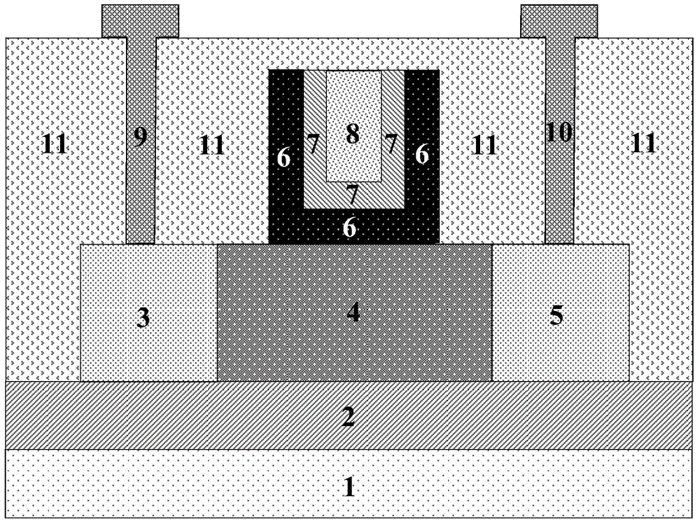
[0039] Such as figure 1 It is a schematic diagram of a two-dimensional structure of an insulated gate tunneling bipolar transistor with a U-shaped tunneling insulating layer formed on an SOI substrate in the present invention; it specifically includes a single crystal silicon substrate 1; a wafer insulating layer 2; an emitter region 3; Region 4; collector region 5; U-shaped conductive layer 6; U-shaped tunnel insulating layer 7; gate electrode 8; emitter 9; collector 10; blocking insulating layer 11.

[0040] In order to achieve the device functions described in the present invention, the core structural features of the IGBT with a U-shaped tunneling insulating layer proposed in the present invention are as follows:

[0041]1. The U-shaped tunneling insulating layer 7 is an insulating layer used to generate tunneling current of the gate electrode, which has the character...


PUM


Abstract

The invention relates to an insulated gate tunneling bipolar transistor with a U-shaped tunneling insulating layer. A gate electrode tunneling current is generated by the U-shaped tunneling insulating layer, and the very sensitive mutual relation between impedance of the tunneling insulating layer and intensity of an internal electric field of the tunneling insulating layer is utilized to enable the U-shaped tunneling insulating layer to implement conversion between a high impedance state and a low impedance state in a very short electric potential change interval of a gate electrode, and thus, compared with the prior art, the insulated gate tunneling bipolar transistor can realize a better switching characteristic; by bipolar amplification, the positive conduction characteristic of a nanoscale insulated gate transistor is obviously improved. The invention also discloses a specific manufacturing method of the insulated gate tunneling bipolar transistor with the U-shaped tunneling insulating layer. Therefore, the working characteristic of a nanoscale integrated circuit unit is obviously improved, and the insulated gate tunneling bipolar transistor and the manufacturing method are suitable for being popularized and applied.

Description

Technical field: [0001] The invention relates to the field of ultra-large-scale integrated circuit manufacturing, and relates to a structure and a manufacturing process of an insulated gate tunneling bipolar transistor with a U-shaped tunneling insulating layer suitable for manufacturing high-performance ultra-high integrated integrated circuits. Background technique: [0002] At present, the continuous shortening of the channel length of metal-oxide-semiconductor field-effect transistors (MOSFETs) in integrated circuit units leads to the deterioration of switching characteristics of the devices and the obvious increase of static power consumption. Although the degradation of the performance of the device can be alleviated by improving the structure of the gate electrode, when the size of the device is further reduced, the performance of the device will deteriorate again. [0003] In order to solve the problem of physical size limit of MOSFETs devices, Tunneling Field Effect...

Claims


Application Information

Patent Timeline
Patent Type & Authority Applications(China)
IPC IPC(8): H01L29/739H01L29/423H01L21/331
CPCH01L29/42364H01L29/66325H01L29/7397
Inventor 刘溪靳晓诗
Owner SHENYANG POLYTECHNIC UNIV
Why Eureka
Try Eureka