Boosting circuit

A technology of boosting circuit and capacitor, which is applied in the direction of electrical components, adjusting electric variables, instruments, etc., can solve the problems of output voltage increase and output voltage cannot be adjusted in a wide range, and achieve high efficiency

Active Publication Date: 2015-04-01
SHANGHAI BEILING
View PDF3 Cites 4 Cited by
  • Summary
  • Abstract
  • Description
  • Claims
  • Application Information

AI Technical Summary

Problems solved by technology

The disadvantage of this structure is that the output voltage cannot be adjusted in a wide range due to the limitation of the minimum conduction time of the power switch tube; in addition, the output terminal is generally connected to a preload to prevent the output voltage from rising when no-load.

Method used


Image

  • Boosting circuit
  • Boosting circuit
  • Boosting circuit

Examples


Embodiment Construction

[0042] Hereinafter, the boost circuit and working principle of the present invention will be described with reference to the accompanying drawings.

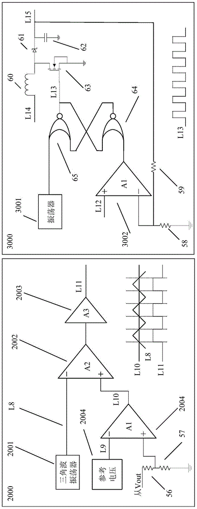
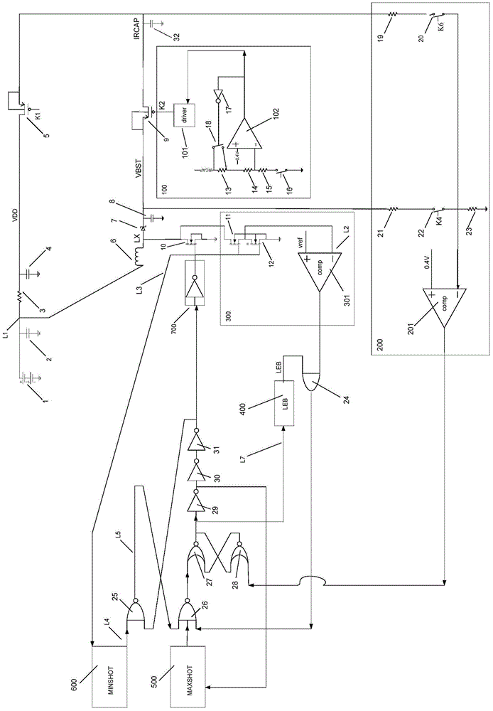
[0043] figure 2 It is a structural diagram of the boost circuit of the present invention. In this implementation manner, a BOOST switching power supply topology is adopted to realize voltage boosting. Using discontinuous mode (DCM), voltage / current feedback.

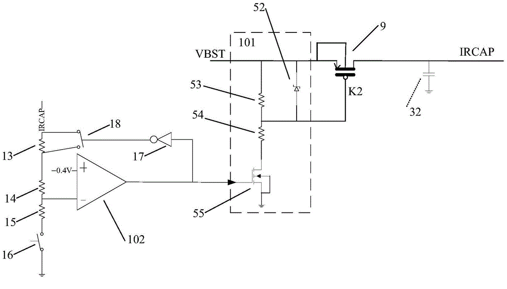
[0044] The bias voltage module has a voltage input node L1 and a voltage output node IRCAP, the voltage input node L1 is connected to the 3V DC voltage source 1 , and the voltage output module IRCAP is grounded through the first capacitor 32 . In this embodiment, a filter circuit and a switch 5 are sequentially connected between the voltage input node L1 and the voltage output node IRCAP, and the filter circuit is composed of an inductor 3 and a capacitor 4 .

[0045]The main boost module is composed of a first power switch tube 10 and an inductance 6, a first diode 7...


PUM


Abstract

The invention relates to a boosting circuit. The boosting circuit comprises a bias voltage module, a main boosting module, a driving control module, a voltage feedback module, a current feedback module, a limiting loop and an oscillating circuit. By utilizing the boosting circuit, a novel boosting modulation structure is provided, and two output voltages are achieved on the basis; moreover, the switching pulse period and the switching pulse frequency are automatically adjusted along with the input output voltage and load conditions, the problem of low loop stability is avoided, and the efficiency is higher.

Description

technical field [0001] The invention belongs to the field of integrated circuit design, in particular to a voltage boosting circuit. Background technique [0002] A switching power supply is a power supply that uses modern power electronics technology to control the time ratio (duty cycle) of switching transistors on and off to maintain a stable output voltage. It can be divided into two categories: AC / DC and DC / DC, and generally consists of a pulse width modulation (PWM) or pulse frequency modulation (PFM) control IC and a power semiconductor device (usually a MOSFET). Such as figure 1 It is the control circuit diagram of PWM modulation mode and PFM modulation mode. [0003] Among them, the module 2000 is a control circuit diagram of the pulse width modulation PWM mode, which is characterized in that the switching frequency is fixed, and the duty cycle is adjusted by changing the pulse width. Its output waveform is that as the amplitude of L10 changes, the pulse width of...

Claims


Application Information

Patent Timeline
Patent Type & Authority Applications(China)
IPC IPC(8): H02M3/156
Inventor 赵海亮刘伟吉丁学欣陈方雄孙彪白晓洁曹志强
Owner SHANGHAI BEILING
Why Eureka
Try Eureka