A method of manufacturing a semiconductor device

A semiconductor and device technology, applied in the field of manufacturing semiconductor devices, can solve problems such as easy breakage of lines, pattern transfer integrity optical proximity correction can not meet the required requirements, etc., to achieve the effect of improving reliability and production efficiency

Active Publication Date: 2017-09-01
SEMICON MFG INT (SHANGHAI) CORP
View PDF4 Cites 0 Cited by
  • Summary
  • Abstract
  • Description
  • Claims
  • Application Information

AI Technical Summary

Problems solved by technology

However, since the current optical proximity correction model (OPC model) is mainly used in the lithography process, the optical proximity correction model combines the optical model (optical model) and the photoresist model (resist model), so in terms of ensuring the integrity of pattern transfer, optical Proximity correction does not meet desired requirements
[0007] Therefore, need a kind of new method, to solve the problem that the line that produces when carrying out the micropattern process of silicon semiconductor substrate is broken easily

Method used


Image

  • A method of manufacturing a semiconductor device
  • A method of manufacturing a semiconductor device
  • A method of manufacturing a semiconductor device

Examples


Embodiment Construction

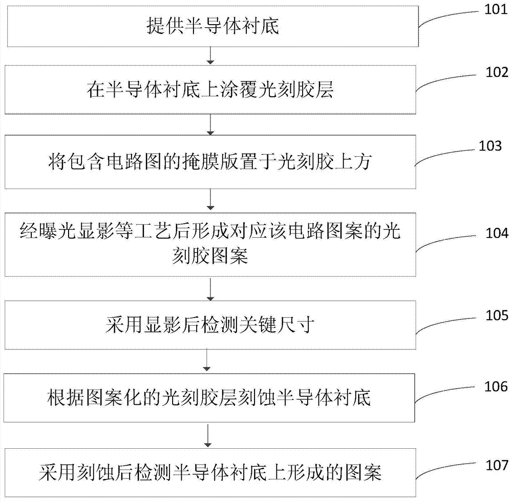
[0021] In the following description, numerous specific details are given in order to provide a more thorough understanding of the present invention. It will be apparent, however, to one skilled in the art that the present invention may be practiced without one or more of these details. In other examples, some technical features known in the art are not described in order to avoid confusion with the present invention.

[0022] In order to thoroughly understand the present invention, detailed steps will be presented in the following description, so as to explain how the present invention improves the process of fabricating semiconductor device structures to solve the problems in the prior art. Obviously, the practice of the invention is not limited to specific details familiar to those skilled in the semiconductor arts. Preferred embodiments of the present invention are described in detail below, however, the present invention may have other embodiments besides these detailed d...


PUM

PropertyMeasurementUnit
lengthaaaaaaaaaa
thicknessaaaaaaaaaa
thicknessaaaaaaaaaa

Abstract

The invention discloses a method for manufacturing a semiconductor device, comprising: providing a design mask, the design mask including a plurality of design main line patterns; Add auxiliary virtual strip pattern at the endpoint of the line pattern, and then obtain the revised design mask; make a photolithography mask according to the modified design mask; use the photolithography mask to process the wafer Photolithography and etching; finally use a cutting mask to cut off unnecessary auxiliary lines according to design needs. According to the method for preparing a semiconductor device of the present invention, the problem that the lines generated during the micropatterning process of the silicon semiconductor substrate are easily broken is solved, so as to ensure that the pattern on the mask plate is completely transferred to the silicon semiconductor substrate, and then The reliability and production efficiency of the prepared semiconductor device structure are improved.

Description

technical field [0001] The invention relates to a semiconductor manufacturing process, in particular to a method for manufacturing a semiconductor device. Background technique [0002] With the increasing maturity of semiconductor integrated circuit (IC) industrial technology and the rapid development of ultra-large-scale integrated circuits, the size of components is getting smaller and smaller, and the integration level of chips is getting higher and higher. Due to the high density of devices, the requirement of small size has an increasingly prominent impact on semiconductor technology. In the existing advanced technology (such as the process generation below 28 nanometers), as the critical dimension of the pattern, that is, the size of the pattern decreases, the speed of the semiconductor device increases, and the integration of the semiconductor device increases. In the micropatterning process (micro-patterning process) is prone to the problem of poly line pinch, which...

Claims


Application Information

Patent Timeline
Patent Type & Authority Patents(China)
IPC IPC(8): H01L21/02G03F1/36G03F7/00
Inventor 舒强张海洋李天慧
Owner SEMICON MFG INT (SHANGHAI) CORP
Why Eureka
Try Eureka