joint assembly device

A technology for assembling devices and metal wires, applied to welding equipment, electrical components, circuits, etc., can solve problems such as hindering heat dissipation, damage to semiconductor devices, and degradation of heat dissipation characteristics, so as to eliminate warping, reduce environmental load, and improve bonding characteristics. Effect

Active Publication Date: 2018-01-30
FUJI ELECTRIC CO LTD
View PDF5 Cites 0 Cited by
  • Summary
  • Abstract
  • Description
  • Claims
  • Application Information

AI Technical Summary

Problems solved by technology

However, if there are air bubbles (voids) in the solder joint layer between the silicon chip and the insulating substrate, or between the insulating substrate and the metal base, these air bubbles hinder heat dissipation, resulting in a significant drop in heat dissipation characteristics , or become the cause of damage to the semiconductor device

Method used


Image

  • joint assembly device
  • joint assembly device
  • joint assembly device

Examples


Embodiment Construction

[0042] Hereinafter, embodiments of the present invention will be described with reference to the drawings. However, the present invention is not limited to the embodiments described below.

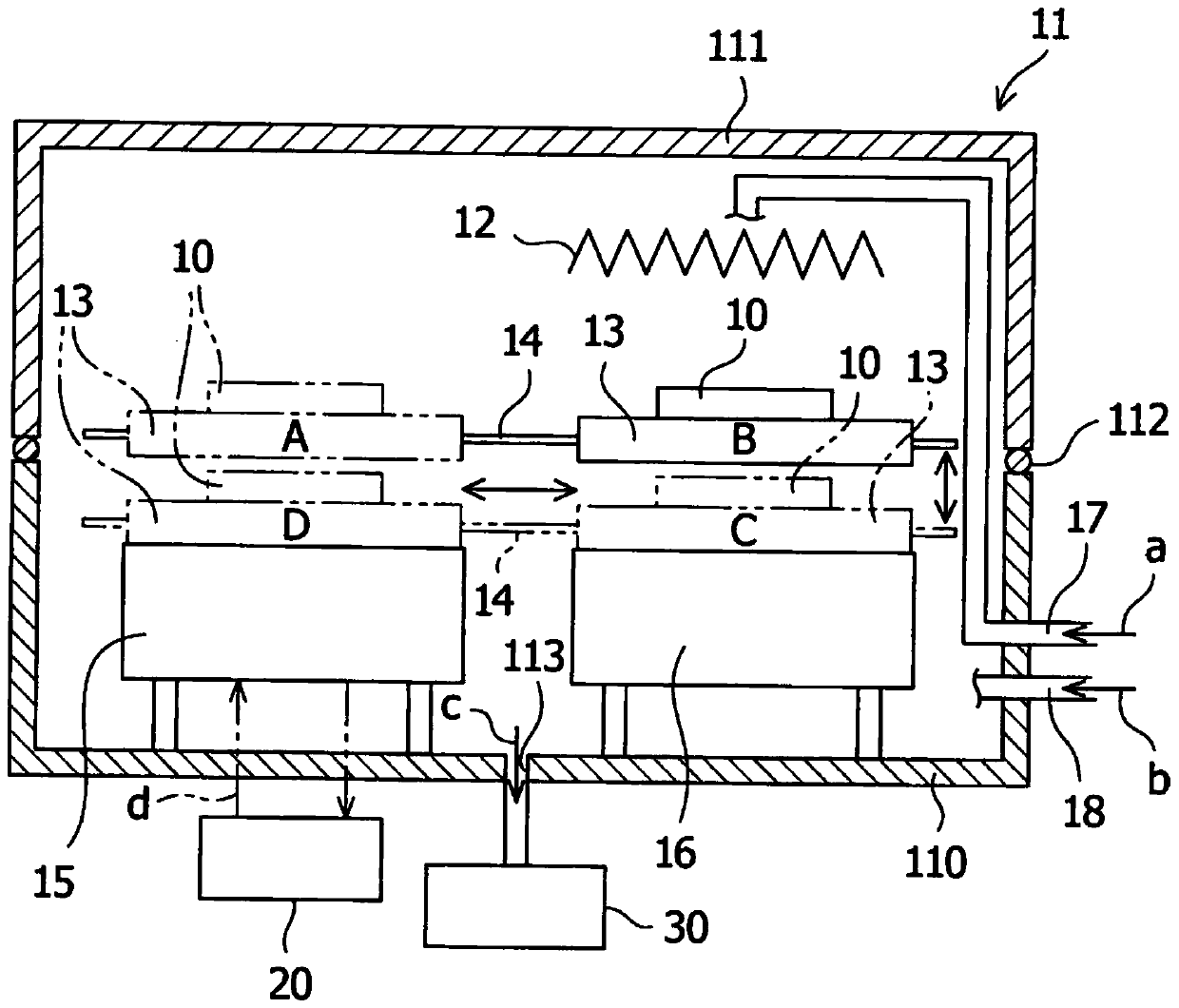
[0043] According to one embodiment of the present invention, the present invention relates to a joint assembly device. figure 1 A schematic diagram of a joint assembly device according to the present invention is shown. The bonding assembly device according to the present invention mainly includes a metal wire 12 , a transfer table 13 , a cooling plate 15 , a hot plate 16 , an active species generation gas introduction pipe 17 , and an inert gas introduction pipe 18 in a reduced pressure furnace 11 . In the present invention, the active species generating gas refers to a gas that is decomposed by contact with the metal wire 12 , has relatively high reducing properties and can generate elements containing unpaired electrons. The above-mentioned active species generating gas is not particu...


PUM

PropertyMeasurementUnit
melting pointaaaaaaaaaa

Abstract

The present invention provides a joining and assembling device that joins a laminated body composed of at least one member to be joined and at least one solder material through a short-time soldering process to obtain a joined body having a solder joint layer with fewer bubbles in the layers. The bonding assembly device includes the following members in the decompression path: a metal wire; a transfer table supporting at least one laminated body of the member to be bonded and at least one welding material, and capable of moving horizontally and vertically; a cooling plate, Cooling the stacked body through the transfer table; hot plate) heating the stacked body through the transfer table; active species gas introduction pipe; inert gas introduction pipe; and exhaust port, the joint The assembly device further includes a heating unit for heating the metal wire by energizing, that is, an unillustrated AC or DC power supply outside the furnace.

Description

technical field [0001] The invention relates to a joint assembly device. In particular, the present invention relates to a bonding and assembling device capable of obtaining a laminate having a solder bonding layer with fewer air bubbles by performing bonding in a short-time soldering process. Background technique [0002] Conventionally, the following three methods have been mainly implemented as methods for manufacturing power semiconductor devices. In the first method, first, pre-soldering is performed using a reducing atmosphere continuous furnace (tunnel furnace), and solder is provided on the back electrode of the silicon chip. Next, the silicon chip is bonded to the insulating substrate using this solder. After that, wire bonding is performed. Then, the insulating substrate on which the silicon chip is soldered is soldered to a metal base made of copper or the like with flux in the atmosphere. [0003] In the second method, a silicon chip and an insulating substra...

Claims


Application Information

Patent Timeline
Patent Type & Authority Patents(China)
IPC IPC(8): H01L21/52B23K1/00
Inventor 斋藤俊介渡边裕彦小野真裕大西一永渡边孝志佐野真二
Owner FUJI ELECTRIC CO LTD
Why Eureka
Try Eureka