
Semiconductor device and method for manufacturing the same

A manufacturing method and semiconductor technology, applied in the fields of semiconductor/solid-state device manufacturing, semiconductor devices, semiconductor/solid-state device components, etc., can solve problems such as reduced bonding life, peeling, and reduced assembly, so as to improve adhesion and inhibit peeling. , the effect of improving reliability

Active Publication Date: 2015-04-15
MITSUBISHI ELECTRIC CORP
View PDF6 Cites 7 Cited by
  • Summary
  • Abstract
  • Description
  • Claims
  • Application Information

AI Technical Summary

Problems solved by technology

[0005] Conventional semiconductor devices are structured as above, so in order to miniaturize the ceramic substrate, it is necessary to reduce the area of ​​the circuit pattern or the width of the insulating part, and there are problems of reduced assembly and insulation
[0006] In addition, in order to suppress the peeling of the epoxy resin, it is necessary to coat the above-mentioned low Young's modulus resin, and since the manufacturing process for coating is increased, there is a problem that the manufacturing cost increases.
If the resin with low Young's modulus is not coated in order to reduce the manufacturing cost, peeling will occur due to the deterioration of the adhesiveness of the epoxy resin
Due to the peeling of the epoxy resin, there are problems such as a decrease in the bonding life of structures held by the epoxy resin (such as aluminum wires, terminals), and a decrease in the insulation between circuit patterns on the ceramic substrate.

Method used


Image

  • Semiconductor device and method for manufacturing the same
  • Semiconductor device and method for manufacturing the same
  • Semiconductor device and method for manufacturing the same

Examples


Embodiment approach 1

[0031]

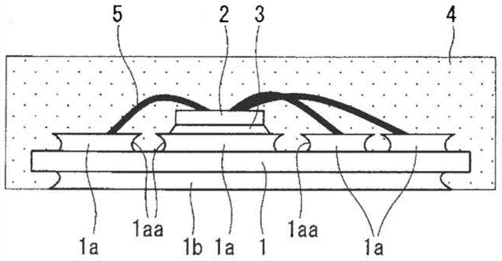
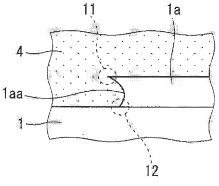
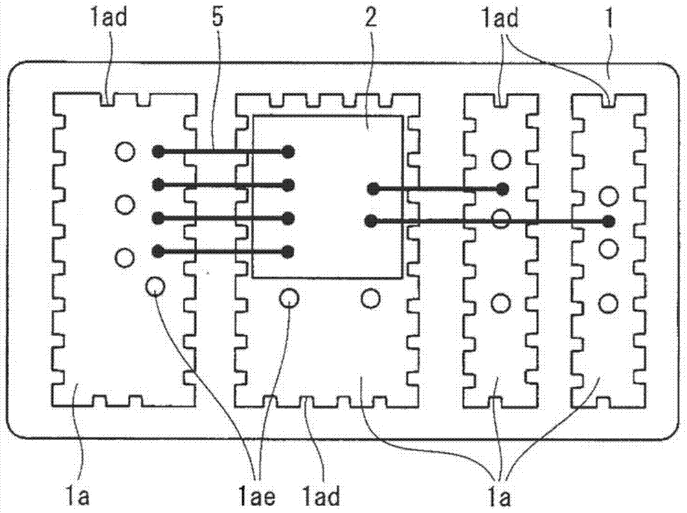
[0032] figure 1 is a cross-sectional view of the semiconductor device of the present embodiment. figure 2 It is a partial enlarged view of the cross section of the semiconductor device of this embodiment. figure 2 In more detail, yes figure 1 The cross-sectional view of the side of the circuit pattern 1a in the cross-sectional view is enlarged. also, image 3 It is a plan view of the semiconductor device of this embodiment.

[0033] In the semiconductor device of this embodiment, a plurality of circuit patterns 1 a are arranged on the surface of a ceramic substrate 1 . The semiconductor element 2 is bonded with solder 3 and mounted on the surface of at least one circuit pattern 1a.

[0034] Such as figure 1 As shown, undercut portions 1aa are formed on opposite side surfaces of circuit patterns 1a adjacent to each other. figure 2 An enlarged view showing the undercut portion 1aa. In the undercut portion 1aa, the end portion 11 of the surface of the circui...

Embodiment approach 2

[0071]

[0072] Figure 8 It is a partial enlarged view of the cross section of the semiconductor device of this embodiment. In the semiconductor device of the present embodiment, the undercut portion 1aa ( figure 2 ) similarly shaped undercuts 1ab. Figure 8 An enlarged view showing the undercut portion 1ab.

[0073] Such as Figure 8 As shown, in the undercut portion 1ab, the end portion 11 of the surface of the circuit pattern 1a protrudes outward compared with the end portion 12 of the surface of the circuit pattern 1a that is in contact with the ceramic substrate 1 . The potting resin 4 is also filled in the undercut portion 1ab. The undercut portion 1aa of Embodiment 1 is an R-shape formed by etching, but the undercut portion 1ab of this embodiment is formed by press working, so it has a linear shape. The other configurations are the same as those in Embodiment 1, and thus descriptions of the same parts are omitted.

[0074]

[0075]A method of manufacturing t...

Embodiment approach 3

[0081]

[0082] Figure 9 It is a partial enlarged view of the cross section of the semiconductor device of this embodiment. In the semiconductor device of the present embodiment, the undercut portion 1aa ( figure 2 ) similarly shaped undercuts 1af. Figure 9 An enlarged view showing the undercut portion 1af.

[0083] Such as Figure 9 As shown, in the undercut portion 1af, the end portion 11 of the surface of the circuit pattern 1a protrudes outward compared with the end portion 12 of the surface of the circuit pattern 1a that is in contact with the ceramic substrate 1 . The potting resin 4 is also filled in the undercut portion 1af.

[0084] Further, on the surface of the circuit pattern 1a, a groove 1ac is formed along the end portion 11 of the surface of the circuit pattern 1a. The distance from the end 11 of the surface of the circuit pattern 1a to the groove 1ac is less than or equal to the thickness of the circuit pattern 1a. In addition, the sealing resin 4 is...


PUM


Abstract

A semiconductor device according to the present invention includes a ceramic substrate, a plurality of circuit patterns arranged on a surface of the ceramic substrate, a semiconductor element arranged on an upper surface of at least one circuit pattern, and a sealing resin for sealing the ceramic substrate, the plurality of circuit patterns, and the semiconductor element, in which an undercut part is formed in opposed side surfaces of the circuit patterns adjacent to one another, the undercut part is configured such that an end of an upper surface of the circuit pattern protrudes outside the circuit pattern more than an end of a lower surface of the circuit pattern on the ceramic substrate, and the undercut part is also filled with the sealing resin.

Description

technical field [0001] The present invention relates to a semiconductor device and a manufacturing method thereof, and to a semiconductor device used in, for example, an inverter for controlling electric motors of electric vehicles and trains, and a converter for regeneration, and a manufacturing method thereof. Background technique [0002] A conventional semiconductor device is composed of a ceramic substrate, a circuit pattern arranged on the ceramic substrate, a semiconductor element mounted on the circuit pattern, and bonding wires connected between the circuit patterns and between the circuit pattern and the semiconductor element. In a semiconductor device, in order to insulate circuit patterns, an insulating portion formed by exposing a ceramic substrate is provided. The size of the ceramic substrate depends on the area of ​​the circuit pattern and the width of the insulating portion. [0003] The ceramic substrate, circuit patterns, semiconductor elements, and bondi...

Claims


Application Information

Patent Timeline
Patent Type & Authority Applications(China)
IPC IPC(8): H01L23/31H01L23/498H01L21/48H01L21/56
CPCH05K3/20H05K1/18H05K2201/09036H05K1/0306H05K3/06H01L2224/32225H01L2224/48091H01L2224/48227H01L2224/73265H01L2924/13055H05K1/0203H05K3/284H05K2201/0373H05K2203/049H05K2203/1184H05K2203/1316H05K2201/2072H01L2224/49175H01L2924/18301H01L2924/00014H01L2924/00
Inventor 吉松直树新饲雅芳鹿野武敏村田大辅木本信义井本裕儿石原三纪夫
Owner MITSUBISHI ELECTRIC CORP
Learn More