Silicon wafer vacuum adsorption manipulator

A vacuum adsorption, manipulator technology, applied in conveyor objects, sustainable manufacturing/processing, electrical components, etc., can solve the problems of high breakage rate, long loading time, high production cost, avoid collision damage and improve production efficiency , the effect of reducing rigid impact

Active Publication Date: 2015-04-22
BEIJING NAURA MICROELECTRONICS EQUIP CO LTD
View PDF5 Cites 10 Cited by
  • Summary
  • Abstract
  • Description
  • Claims
  • Application Information

AI Technical Summary

Problems solved by technology

[0002] The rapid development of solar photovoltaics has put forward higher and higher requirements for automatic wafer rewinding equipment, especially in the core process equipment diffusion furnace. How to solve the automatic loading and unloading of silicon wafers on quartz boats has become an increasingly urgent requirement for production enterprises. At present, the loading and unloading of quartz boats in the photovoltaic cell production line is mainly completed by manual insertion of a single piece with a vacuum pen. There are 250 slots on the quartz boat, the slot distance is 4.76mm, and the thickness of the silicon wafer is 180μm. It is necessary to insert the silicon wafer back to back. In the quartz boat slot, loading and unloading 500 pieces at a time requires high proficiency of workers. The whole process is monotonous and repetitive, and the flow of personnel is very high, which brings great difficulty to production management, and the loading time is long and the damage rate is high. , High production cost, which is not conducive to the large-scale promotion of the entire cell production
Large-scale enterprises use offline rewinders, but they cannot achieve seamless connection with online automatic production lines in assembly operations, and thus cannot achieve efficient online automatic production

Method used


Image

  • Silicon wafer vacuum adsorption manipulator
  • Silicon wafer vacuum adsorption manipulator
  • Silicon wafer vacuum adsorption manipulator

Examples


Embodiment 1

[0041] The present invention provides a silicon chip vacuum adsorption manipulator, comprising: a rotating power device 1, a mounting bracket 2, a detection device 6, a vacuum chamber 7 with a vacuum pipeline inside, and a comb-shaped vacuum adsorption finger 8;

[0042] The rotating power device 1 and the detection device 6 are fastened on the mounting bracket 2 by a fastening device;

[0043] The output shaft of the rotating power device 1 is firmly connected with the upper end surface of the vacuum chamber 7;

[0044] The detection device 6 includes several position sensors 12 that feed back position information for precisely positioning the rotational movement of the floating support 4;

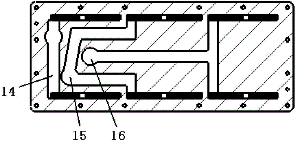
[0045] The vacuum chamber 7 is provided with a pipe joint 17 communicating with the vacuum pipeline;

[0046] The comb-tooth-shaped vacuum suction finger 8 is internally provided with independent vacuum pumping pipelines that are consistent with the number of comb-tooth gaps; The upper ...

Embodiment 2

[0052] The present invention provides a vacuum adsorption manipulator for silicon wafers, comprising: a rotating power device 1, a mounting bracket 2, a rotating mechanism 3, a detection device 6, a vacuum chamber 7 with a vacuum pipeline inside, and a comb-shaped vacuum adsorption finger 8;

[0053] The rotating power device 1, the rotating mechanism 3 and the detection device 6 are fastened on the mounting bracket 2 by a fastening device;

[0054] A speed reducer 9 is fastened inside the rotating mechanism 3; the output shaft of the rotating power unit 1 realizes transmission connection with the input shaft of the speed reducer 9 through a transmission device;

[0055] The output shaft of the reducer 9 is fastened to the upper end surface of the vacuum chamber 7 through a connecting piece;

[0056] The detection device 6 includes several position sensors 12 that feed back position information for precisely positioning the rotational movement of the floating support 4;

[00...

Embodiment 3

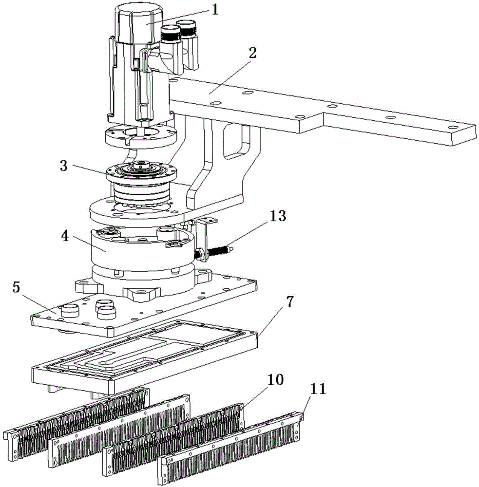
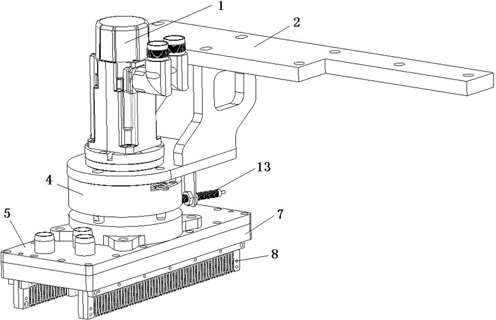
[0062] Figure 1~4 As shown, the present invention provides a vacuum adsorption manipulator for silicon wafers comprising: a precision rotating power device 1, a mounting bracket 2, a rotating mechanism 3, a sealing cover 5, a detection device 6, a vacuum chamber 7 and a comb-shaped vacuum adsorption finger 8 ;

[0063] The precision rotating power device 1, the rotating mechanism 3 and the detection device 6 are fastened on the mounting bracket 2 by a fastening device;

[0064] A precision reducer 9 is fastened inside the rotating mechanism 3; the output shaft of the precision rotating power device 1 is connected to the input shaft of the precision reducer 9 through a transmission device;

[0065] The output shaft of the precision reducer 9 is tightly connected to the upper end surface of the sealing cover plate 5 through a connecting piece;

[0066] The detection device 6 includes several position sensors 12 that feed back position information for precisely positioning the...


PUM


Abstract

The invention relates to the technical field of crystalline silicon solar cell automatic production equipment, in particular to a silicon wafer vacuum adsorption manipulator. A manipulator capable of conveying silicon wafers stably and efficiently is provided for online automatic production. The side faces of comb-shaped grooves of comb-shaped vacuum adsorption fingers are concave-convex adsorption surfaces, so that the adsorption area is increased, and the effect of preventing the silicon wafers from being broken is achieved. Through adoption of the manipulator, a plurality of silicon wafers can be stably adsorbed in vacuum, and can be accurately rotated horizontally by preset angles. Furthermore, 50 silicon wafers can be adsorbed at a time and can be rotated by 180 degrees, and 100 silicon wafers are automatically placed together back to back.

Description

technical field [0001] The invention relates to the technical field of automatic production equipment for crystalline silicon solar cells, in particular to a silicon wafer vacuum adsorption manipulator. Background technique [0002] The rapid development of solar photovoltaics has put forward higher and higher requirements for automatic wafer rewinding equipment, especially in the core process equipment diffusion furnace. How to solve the automatic loading and unloading of silicon wafers on quartz boats has become an increasingly urgent requirement for production enterprises. At present, the loading and unloading of quartz boats in the photovoltaic cell production line is mainly completed by manual insertion of a single piece with a vacuum pen. There are 250 slots on the quartz boat, the slot distance is 4.76mm, and the thickness of the silicon wafer is 180μm. It is necessary to insert the silicon wafer back to back. In the quartz boat slot, loading and unloading 500 pieces ...

Claims


Application Information

Patent Timeline
Patent Type & Authority Applications(China)
IPC IPC(8): H01L21/67H01L21/677H01L21/683H01L31/18
CPCH01L21/677H01L21/6838H01L31/18Y02P70/50
Inventor 李旭刚郝晓明宋晓彬王广明
Owner BEIJING NAURA MICROELECTRONICS EQUIP CO LTD
Why Eureka
Try Eureka