Method for manufacturing energy-accumulation photoelectricity CIGS solar cell
A solar cell and optoelectronic technology, applied in the fields of photovoltaic power generation, circuits, electrical components, etc., can solve the problems of not easy to carry, limit the development of miniaturization of solar cells, etc., and achieve the effect of increasing electrical conductivity
- Summary
- Abstract
- Description
- Claims
- Application Information
AI Technical Summary
Problems solved by technology
Method used
Image
Examples
Embodiment 1
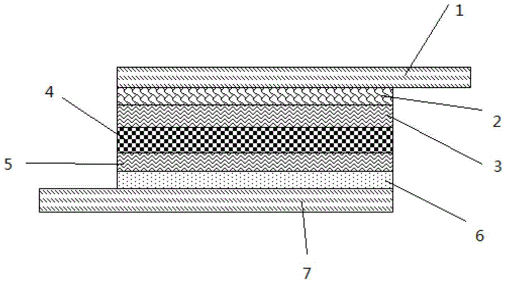
[0024] Sputter 0.45g of copper, 0.15g of indium, 0.35g of gallium and 1g of carbon microspheres onto the conductive surface of the top conductive glass substrate 1 by hybrid sputtering at 200°C, and then perform selenization in a selenium atmosphere to form For the CIGS storage layer 2 with a thickness of 500 μm, in the process of mixed sputtering and selenization, the mass ratio of copper: indium: gallium: selenium: carbon microspheres is 9:3:7:15:20;
[0025] Spray metal oxide NiO on the bottom conductive glass substrate 7, sinter at 300°C to form the storage layer 6, insert the separator 4 between the CIGS storage layer 2 and the storage layer 6, and press them, and then press them Tetraethylammonium tetrafluoroborate and dimethyl carbonate are injected into the device at a volume ratio of 1:1 to form the first electrolyte layer 3 and the second electrolyte layer 5 respectively, and then seal the periphery of the device to form an energy storage Photovoltaic CIGS solar cell...
Embodiment 2
[0028] Sputter 0.45g copper, 0.15g indium, 0.35g gallium and 1.2g carbon microspheres onto the conductive surface of the top conductive glass substrate 1 by hybrid sputtering method at 200°C, and then perform selenization under a selenium atmosphere A CIGS storage layer 2 with a thickness of 700 μm is formed. During the mixed sputtering and selenization process, the mass ratio of copper: indium: gallium: selenium: carbon microspheres is 9:3:7:15:24;
[0029] Spray polyaniline on the conductive glass substrate 7 on the bottom surface, sinter at 300°C to form the storage layer 6, insert the separator 4 between the CIGS storage layer 2 and the storage layer 6, and press them, and then put them into the pressed device Inject monomethyltriethylammonium tetrafluoroborate and dimethyl carbonate at a volume ratio of 1:1 to form the first electrolyte layer 3 and the second electrolyte layer 5 respectively, and then seal the periphery of the device to form a reservoir. Energy photoelect...
Embodiment 3
[0032] Sputter 0.45g copper, 0.15g indium, 0.35g gallium and 1.4g carbon microspheres onto the conductive surface of the top conductive glass substrate 1 by hybrid sputtering method at 300°C, and then perform selenization under a selenium atmosphere A CIGS storage layer 2 with a thickness of 900 μm is formed, and in the process of mixed sputtering and selenization, the mass ratio of copper: indium: gallium: selenium: carbon microspheres is 9:3:7:15:28;
[0033] Spraying metal oxide MnO on the bottom conductive glass substrate 7 2 , sintered at 300°C to form the storage layer 6, insert the separator 4 between the CIGS storage layer 2 and the storage layer 6 and press them, and then inject tetraethyl into the pressed device at a volume ratio of 1:1 Ammonium tetrafluoroborate and diethyl carbonate form the first electrolyte layer 3 and the second electrolyte layer 5 respectively, and then seal the periphery of the device to form an energy storage photoelectric CIGS solar cell.
...
PUM
| Property | Measurement | Unit |
|---|---|---|
| thickness | aaaaa | aaaaa |
| thickness | aaaaa | aaaaa |
| thickness | aaaaa | aaaaa |
Abstract
Description
Claims
Application Information
 - R&D Engineer
- R&D Manager
- IP Professional
- Industry Leading Data Capabilities
- Powerful AI technology
- Patent DNA Extraction
Browse by: Latest US Patents, China's latest patents, Technical Efficacy Thesaurus, Application Domain, Technology Topic, Popular Technical Reports.
© 2024 PatSnap. All rights reserved.Legal|Privacy policy|Modern Slavery Act Transparency Statement|Sitemap|About US| Contact US: help@patsnap.com


