Electronic skin and production method thereof

A technology of electronic skin and manufacturing method, which is applied in the field of sensors, can solve the problems of low sensitivity, high working voltage, and high power consumption, and achieve the effects of high sensitivity, low power consumption, and good stability

Inactive Publication Date: 2015-04-29
SUZHOU INST OF NANO TECH & NANO BIONICS CHINESE ACEDEMY OF SCI
View PDF5 Cites 37 Cited by
  • Summary
  • Abstract
  • Description
  • Claims
  • Application Information

AI Technical Summary

Problems solved by technology

[0005] The purpose of the present invention is to provide an electronic skin and its manufacturing method, whi

Method used


Image

  • Electronic skin and production method thereof
  • Electronic skin and production method thereof
  • Electronic skin and production method thereof

Examples


Embodiment Construction

[0031] The technical solutions in the embodiments of the present invention will be described in detail below in conjunction with the accompanying drawings in the embodiments of the present invention. Obviously, the described embodiments are only some of the embodiments of the present invention, not all of them. Based on the embodiments of the present invention, all other embodiments obtained by persons of ordinary skill in the art without making creative efforts belong to the protection scope of the present invention.

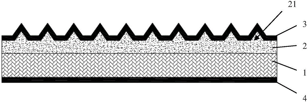
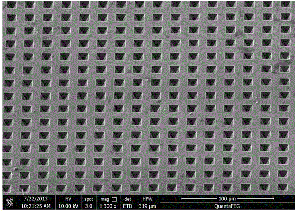
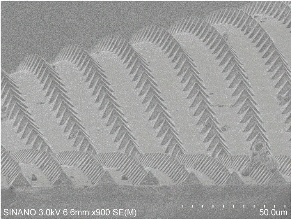
[0032] ginseng figure 1 As shown, the electronic skin in this embodiment includes a flexible support layer 1, a flexible sensitive layer 2 formed on the upper surface of the support layer 1, and an upper electrode layer respectively formed on the upper surface of the sensitive layer 2 and the lower surface of the support layer 1 3 and the lower electrode layer 4.

[0033] The material of the sensitive layer 2 is preferably PDMS (polydimethylsiloxane), and the ...


PUM

PropertyMeasurementUnit
Thicknessaaaaaaaaaa
Thicknessaaaaaaaaaa
Heightaaaaaaaaaa

Abstract

The application discloses an electronic skin, which comprises a flexible sensitive layer, wherein at least one of the upper surface and lower surface of the sensitive layer is of a nonplanar structure, and an upper electrode layer and a lower electrode layer are respectively formed on the upper surface and lower surface of the sensitive layer. The invention also discloses a fabrication method for the electronic skin. The electronic skin disclosed by the invention is integrated with a novel micro/nano sensing technology, the electronic skin can be perfectly integrated with the skin of the human body because an ultrathin elastic film material which is nontoxic and has good biocompatibility is used, and therefore a formed wearable device can bring excellent experience to a user; meanwhile, because of the unique nanostructure of the sensitive material, the device has higher sensitivity and better stability; in addition, because the whole device is light and small, the device has the advantage of convenience in carrying.

Description

technical field [0001] The invention belongs to the field of sensors, in particular to an electronic skin and a manufacturing method thereof. Background technique [0002] As human beings, our direct interaction with the surrounding environment is achieved through our senses and skin. In the field of artificial intelligence, the technology of electronically realizing bionic touch functions is still a huge challenge. The emergence and development of electronic skin is expected It plays a vital role in the realization of bionic touch function in the field of artificial intelligence. Since the OFET electronic skin was first proposed by the University of Tokyo in 2004, capacitive, piezoresistive, piezoelectric and other electronic skins have been successfully constructed. In recent years, with the rapid development of nanomaterials and nanotechnology, artificial electronic skin based on nanomaterials and nanostructures has shown excellent performance such as high sensitivity, f...

Claims


Application Information

Patent Timeline
IPC IPC(8): B81B3/00B82B3/00
Inventor 张珽熊作平王学文顾杨谷文
Owner SUZHOU INST OF NANO TECH & NANO BIONICS CHINESE ACEDEMY OF SCI
Why Eureka
Try Eureka