Integrated narrowband micro light filter
A kind of optical filter, miniature technology, applied in the field of optical filter
- Summary
- Abstract
- Description
- Claims
- Application Information
AI Technical Summary
Problems solved by technology
Method used
Image
Examples
Embodiment 1
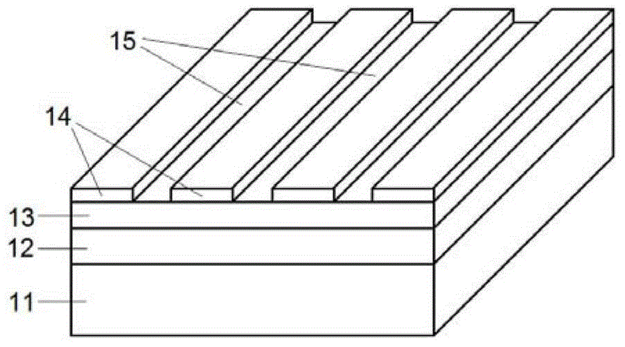
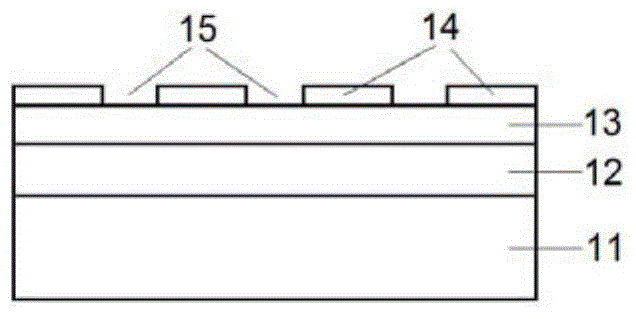
[0024] see figure 1 and 2 , present embodiment 1 is provided with substrate 11, is provided with one layer of dielectric thin film layer 12 with relatively high refractive index on substrate 11, is provided with one layer of dielectric thin film layer with relatively lower refractive index on dielectric thin film layer 12 13. A layer of periodic one-dimensional metal grating 14 is arranged on the dielectric thin film layer 13, and there are gaps 15 between the metal strips of the metal grating 14. The substrate 11 is selected from a transparent dielectric substrate or a semiconductor substrate (the semiconductor substrate can be the semiconductor base material used to make the involved optoelectronic devices). The dielectric thin film layer 12 selects insulating media such as silicon nitride, aluminum oxide, or other semiconductor materials with low absorption and high transmittance in the light band involved; the dielectric thin film layer 12 can also be a semiconductor opto...
Embodiment 2
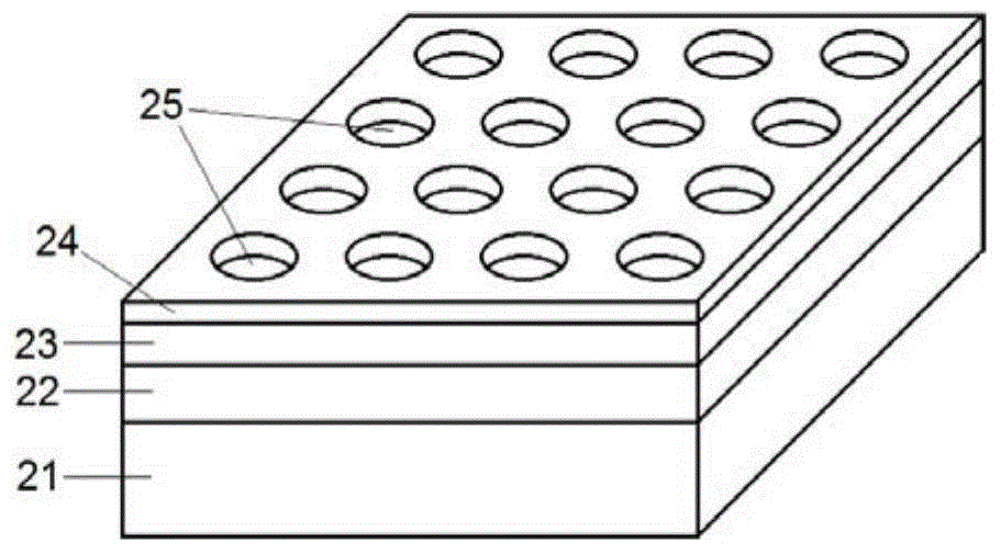
[0026] see image 3 , similar to Example 1. The difference is that the metal grating is a mesh two-dimensional metal grating. The present embodiment 2 is provided with a substrate 21, on the substrate 21 is provided with a dielectric film layer 22 with a relatively high refractive index, on the dielectric film layer 22 there is a dielectric film layer 23 with a relatively low refractive index, On the dielectric thin film layer 23 there is a layer of periodic mesh two-dimensional metal grating 24 , and there are holes 25 in the mesh two-dimensional metal grating 24 . In this embodiment, the material selection of the substrate 21, the dielectric thin film layer 22, the dielectric thin film layer 23, and the two-dimensional metal grating 24 are respectively the same as those of the substrate 11, the dielectric thin film layer 12, the dielectric thin film layer 13, and the one-dimensional metal grating in Embodiment 1. The choice of material for the grating 14 is the same.
[0...
Embodiment 3
[0029] see Figure 4 , similar to Example 1. The difference is that the metal grating is an island-shaped two-dimensional metal grating. The present embodiment 3 is provided with a substrate 31, on the substrate 31 is provided with a dielectric thin film layer 32 with a relatively high refractive index, on the dielectric thin film layer 32 there is a dielectric thin film layer 33 with a relatively low refractive index, On the dielectric thin film layer 33 there is a layer of periodic island-shaped two-dimensional metal grating 34 . In this embodiment, the material selection of the substrate 31, the dielectric film layer 32, the dielectric film layer 33, and the two-dimensional metal grating 34 are respectively the same as those of the substrate 11, the dielectric film layer 12, the dielectric film layer 13, and the one-dimensional metal grating in Embodiment 1. The choice of material for the grating 14 is the same.
[0030] The selection range of the structural size of each...
PUM
| Property | Measurement | Unit |
|---|---|---|
| Thickness | aaaaa | aaaaa |
| Thickness | aaaaa | aaaaa |
Abstract
Description
Claims
Application Information


