Film transistor and manufacturing method thereof

A technology of thin film transistors and manufacturing methods, which is applied in the direction of transistors, semiconductor/solid-state device manufacturing, semiconductor devices, etc., can solve the problems of inability to meet the on-state current requirements of AMOLED, increase the complexity of the manufacturing process, and low carrier concentration, and achieve Reduce the number of process photomasks, save the number of ion implantations, and have good process compatibility

Active Publication Date: 2015-04-29
KUNSHAN GO VISIONOX OPTO ELECTRONICS CO LTD
View PDF4 Cites 13 Cited by
  • Summary
  • Abstract
  • Description
  • Claims
  • Application Information

AI Technical Summary

Problems solved by technology

However, in the existing process of manufacturing LTPS-TFT, for undoped p-Si, the carrier concentration is low, resulting in low mobility, which cannot meet the requirements of AMOLED for TFT on-state current
In addition, ion implantation is also used for heavy doping to form an ohmic contact between the source / drain and p-Si, or a lightly doped drain (Lightly Doped Drain, LDD) structure. However, these methods require at least three different doses Doping, and at least one mask process is added, thus increasing the complexity of the manufacturing process

Method used


Image

  • Film transistor and manufacturing method thereof
  • Film transistor and manufacturing method thereof
  • Film transistor and manufacturing method thereof

Examples


no. 1 example

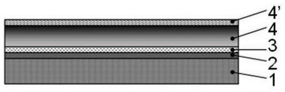
[0030] Figure 1A to Figure 1E It is a schematic diagram of the manufacturing process of the thin film transistor according to the first embodiment of the present invention.

[0031] refer to Figure 1A As shown, buffer layers 2 and 3 are sequentially deposited on a substrate 1 . The material of the substrate 1 can be glass, quartz, organic polymer, or opaque / reflective material. The buffer layers 2 and 3 can be formed by a low-pressure chemical vapor deposition process or an ion-increased chemical vapor deposition process. The buffer layer can prevent impurities contained in the substrate from entering the polysilicon layer 41 . In a specific embodiment, the buffer layer may be a single layer of silicon oxide or a double layer structure of silicon oxide / silicon nitride. Then deposit an amorphous silicon layer on the buffer layers 2 and 3, and crystallize the amorphous silicon layer. The crystallization method can be selected from any one of excimer laser crystallization, so...

no. 2 example

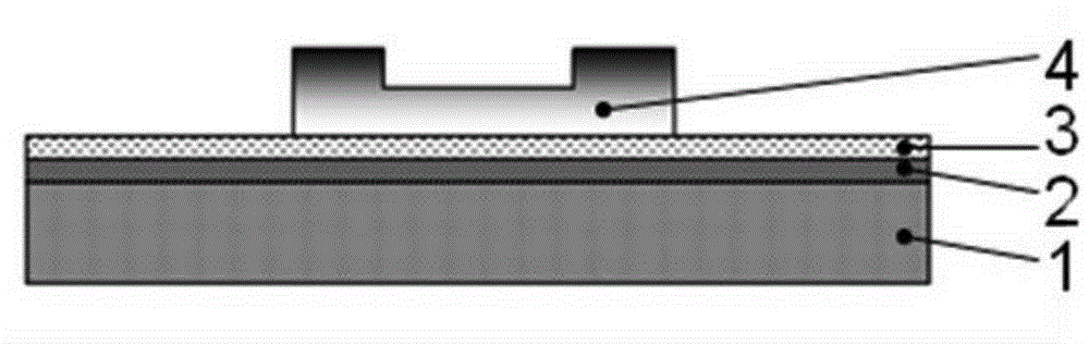
[0039] Figure 2A to Figure 2E It is a schematic diagram of the manufacturing process of the thin film transistor according to the second embodiment of the present invention.

[0040] refer to Figure 2AAs shown, buffer layers 2 and 3 are sequentially deposited on a substrate 1 . Then a first amorphous silicon layer is deposited on the buffer layers 2 and 3, and the first amorphous silicon layer is crystallized. The first amorphous silicon layer is transformed into a polysilicon layer 41 after crystallization. The difference between the second embodiment and the first embodiment is that the second amorphous silicon layer 42 is deposited before the barrier layer 4' is deposited on the polysilicon layer 41. Preferably, the thickness of the second amorphous silicon layer 42 is 1-5000 ?, the thickness of the polysilicon layer is 1~5000 ?. Because in the crystallization process, if the polysilicon layer 41 is too thick, it is not conducive to generating polysilicon with good un...

no. 3 example

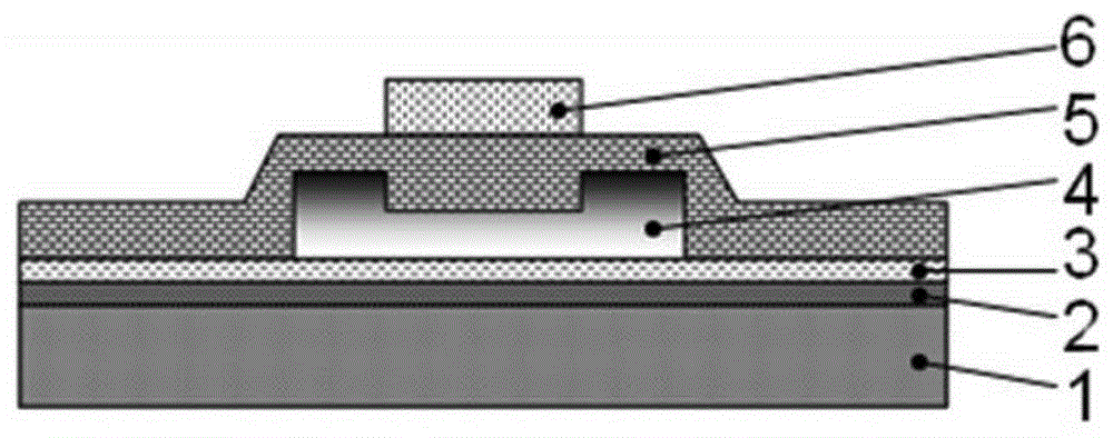
[0043] Figure 3A to Figure 3E It is a schematic diagram of the manufacturing process of the thin film transistor according to the third embodiment of the present invention.

[0044] The difference between this embodiment and the previous two embodiments lies in the method of forming the polysilicon layer whose dopant ion concentration is distributed in a gradient from high to low from the upper surface to the lower surface. refer to Figure 3A As shown, buffer layers 2 and 3 are sequentially deposited on substrate 1 . Then, an ion-enhanced chemical vapor deposition process (Plasma Enhanced Chemical Vapor Deposition, PECVD) is used to deposit an amorphous silicon layer on the buffer layer. While depositing the amorphous silicon layer 4, a dopant gas is introduced. For the p-type channel B-containing gas can be introduced, and P or As-containing gas can be introduced for N-type doping, and the concentration of doping gas is controlled to gradually increase, and finally the co...


PUM


Abstract

The invention discloses a film transistor and a manufacturing method thereof. The manufacturing method comprises the following steps: manufacturing a buffer layer on a substrate; manufacturing a polycrystalline silicon layer after ion doping on the buffer layer, wherein the concentrations of doped ions of the polycrystalline silicon layer after ion doping is distributed in a high-to-low gradient manner from the upper surface to the lower surface of the polycrystalline silicon layer; etching the polycrystalline silicon layer to form a concave silicon island, wherein the sunken part of the concave silicon island is a channel region, and a convex part is a source drain region; successively forming a gate-insulation layer, a gate layer, an interlayer insulation layer and a source drain electrode on the concave silicon island. The film transistor and the manufacturing method thereof, disclosed by the invention, have the advantages that an ion implantation technology is adopted, or the doping concentration is controlled in a PECVD (plasma enhanced chemical vapor deposition) technology, so that the purpose of the vertical gradient of the density of the doped ions is realized, and the number of times of implanting the ions is omitted or reduced; besides, the number of photomasks in a film transistor technology can be reduced, and the process complexity is reduced; in addition, the vertical concentration gradient can form an LDD (laser detector diode) structure, so that TFT (thin film transistor) leak currents are reduced.

Description

technical field [0001] The invention relates to the field of semiconductors, and particularly designs a thin film transistor and a manufacturing method thereof. Background technique [0002] Thin-film transistors are widely used in daily life as driving elements in liquid crystal displays. Generally speaking, thin-film transistors have at least gate, source, drain, and channel components, among which the voltage of the gate can be controlled To change the conductivity of the channel, so that the source and the drain are in a state of conduction (on) or insulation (off). In addition, an N-type or P-type doping is usually formed on the channel. The impurity ohmic contact layer is used to reduce the contact resistance between the channel and the source or between the channel and the drain. [0003] Low Temperature Poly-silicon Thin Filmtransistor (LTPS TFT) has the characteristics of low power consumption and low electromagnetic interference, and has great advantages in compon...

Claims


Application Information

Patent Timeline
Patent Type & Authority Applications(China)
IPC IPC(8): H01L21/336H01L29/786H01L29/06H01L29/08H01L29/10
CPCH01L29/0684H01L29/0847H01L29/105H01L29/66757H01L29/78621H01L29/78672H01L29/78696H01L2029/7863
Inventor 王迪
Owner KUNSHAN GO VISIONOX OPTO ELECTRONICS CO LTD
Why Eureka
Try Eureka