
Technology integration method of fin field-effect transistor

A field effect transistor and process technology, applied in the field of process integration of fin field effect transistors, can solve problems such as unfavorable fin layer target layer etching and flattening process, inability to monitor thickness online, limiting device flexibility, etc., and achieve improvement Uniformity and fin layer etch uniformity, protection of film thickness measurement marks, effect of improving flexibility

Inactive Publication Date: 2015-04-29
SHANGHAI INTEGRATED CIRCUIT RES & DEV CENT
View PDF5 Cites 2 Cited by
  • Summary
  • Abstract
  • Description
  • Claims
  • Application Information

AI Technical Summary

Problems solved by technology

[0003] However, the fin layer patterning process using the side wall hard mask self-aligned patterning has the following disadvantages: first, the formed fin layer pattern has a single size
Therefore, different device channel widths cannot be defined by changing the width of the fin layer, or different devices can only be defined by changing the number of fins
This places high demands on the design rules and also limits the flexibility of the device
Second, because the thickness of the sidewall hard mask is very thin, the width of the formed fin layer pattern is very small, and no matter the size of the core layer pattern area, the final pattern can only be left in the area of ​​the peripheral sidewall
Therefore, the pattern density formed by the side wall hard mask is very low, which is not conducive to the etching of the target layer of the fin layer and the planarization process after the deposition of the insulating layer of the fin layer.
Third, sidewall hard mask self-aligned patterning techniques can destroy markings for in-line monitoring and measurement
For example, thickness measurement marks, etc., require large graphics with a certain area. However, after the fin layer patterning process, only the graphics in the area where the side walls are located are left, and there are no large graphics with a certain area, so online thickness monitoring cannot be performed.

Method used


Image

  • Technology integration method of fin field-effect transistor
  • Technology integration method of fin field-effect transistor
  • Technology integration method of fin field-effect transistor

Examples


Embodiment Construction

[0026] The specific embodiment of the present invention will be further described in detail below in conjunction with the accompanying drawings.

[0027] It should be noted that, in the following specific embodiments, when describing the embodiments of the present invention in detail, in order to clearly show the structure of the present invention for the convenience of description, the structures in the drawings are not drawn according to the general scale, and are drawn Partial magnification, deformation and simplification are included, therefore, it should be avoided to be interpreted as a limitation of the present invention.

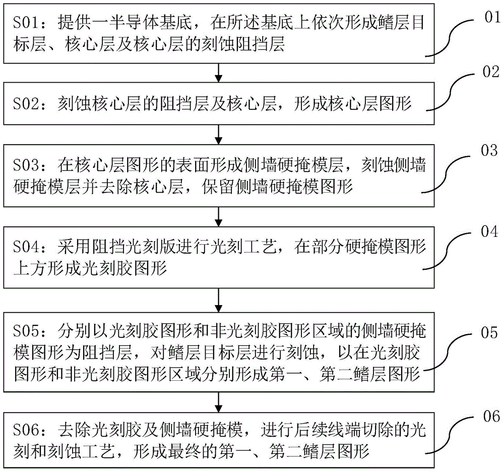
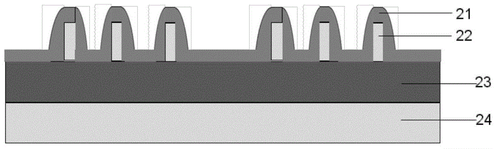
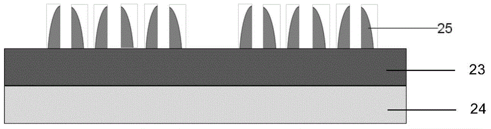
[0028] In the following specific embodiments of the present invention, please refer to figure 1 , and see in conjunction with Figure 2 to Figure 5 . in, figure 1 It is a flow chart of a fin field effect transistor process integration method of the present invention, Figure 2 to Figure 5 is based on figure 1 Schematic diagram of the structure o...


PUM


Abstract

The invention discloses a technology integration method of a fin field-effect transistor. After side wall etching and core layer removing in a fin layer patterning technology process, a barrier photoetching model is additionally adopted for performing a photoetching technology, and a virtual pattern for improving the planarization of a fin layer insulating layer, fin layer patterns different from a non-photoresist pattern region in width, a protecting pattern for measuring marks and other patterns contained in the barrier photoetching model are utilized to increase the density of final fin layer patterns, improve the flexibility of fin layer layout design and obtain the fin layer patterns different in width. Thus, on the premise of limited cost increase, multiple devices can be manufactured on a silicon wafer substrate, the uniformity of a follow-up fin layer insulating layer planarization technology and the uniformity of fin layer etching can be improved, and the film thickness measuring marks can be protected.

Description

technical field [0001] The invention relates to the technical field of integrated circuit manufacturing, and more specifically, to a process integration method for fin field effect transistors. Background technique [0002] Fin Field Effect Transistor (FinFET) technology is the next frontier in the integrated circuit industry. FinFET is a brand-new multi-gate three-dimensional transistor, and its active layer is also called fin layer. In the patterning process of the FinFET fin layer, due to the characteristics of the design rules and the limitation of the resolution of the lithography machine, two photolithography plates and two photolithography processes are generally used, and the side wall hard mask is used to automatically Align patterning technology and line end cutting patterning technology to form the final fin layer patterning process. [0003] However, the process of patterning the fin layer by self-alignment patterning of the sidewall hard mask has the following...

Claims


Application Information

Patent Timeline
Patent Type & Authority Applications(China)
IPC IPC(8): H01L21/336H01L29/78
CPCH01L29/66795
Inventor 袁伟李铭
Owner SHANGHAI INTEGRATED CIRCUIT RES & DEV CENT
Features
  • Generate Ideas
  • Intellectual Property
  • Life Sciences
  • Materials
  • Tech Scout
  • Unparalleled Data Quality
  • Higher Quality Content
  • 60% Fewer Hallucinations
Learn More