Side-illuminated pin photodetector chip and manufacturing method thereof

A photodetector and manufacturing method technology, applied in the field of optical communication transmission, can solve the problems of large chip capacitance and distribution parameters, long drift time, butt coupling of passive optical waveguides, etc., achieve good butt coupling, reduce distribution parameters, ensure The effect of side light mode

Active Publication Date: 2016-01-06
SHENZHEN PHOGRAIN INT TECH DEV
View PDF6 Cites 0 Cited by
  • Summary
  • Abstract
  • Description
  • Claims
  • Application Information

AI Technical Summary

Problems solved by technology

However, if figure 1 and figure 2 As shown, the current conventional PIN photodetector chip adopts a conventionally designed epitaxial wafer 100, and the photogenerated carriers generated after the PIN photodetector chip receives light have a longer drift time in the PN junction of the chip, and a larger diffusion source area 200 and planar structure design, resulting in relatively large chip capacitance and distribution parameters, resulting in the receiving rate of the PIN photodetector chip cannot reach 28G
In addition, the light-receiving surface of the current common photodetector chip is on the front or back of the chip, such as figure 1 The photosensitive surface in 300 and as figure 2 The photosensitive surface 400 in the chip cannot be directly coupled with the passive optical waveguide, so it cannot be used to form an optical receiving chip with a receiving rate of 100G

Method used


Image

  • Side-illuminated pin photodetector chip and manufacturing method thereof
  • Side-illuminated pin photodetector chip and manufacturing method thereof
  • Side-illuminated pin photodetector chip and manufacturing method thereof

Examples


Embodiment Construction

[0039] The present invention will be described in detail below in conjunction with the accompanying drawings and specific embodiments.

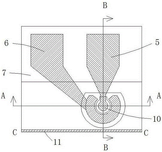
[0040] see Figure 3 to Figure 12 , the present invention provides a side-illuminated PIN photodetector chip, comprising: a substrate 12, a buffer layer 13 formed on the substrate 12, an absorbing layer 14 formed on the buffer layer 13, formed on The transition layer 15 on the absorption layer 14, the top layer 16 formed on the transition layer 15, the contact layer 17 formed on the top layer 16, the substrate 12, the buffer layer 13 and the contact layer 17 The composite passivation layer 19 on the composite passivation layer 19, the first protection layer 7 formed on the composite passivation layer 19, the negative electrode 6 formed on the first protection layer 7, the composite passivation layer 19 and the buffer layer 13, The positive electrode 5 formed on the contact layer 17, the composite passivation layer 19 and the first protective...


PUM


Abstract

The invention discloses a lateral light incidence type PIN photoelectric detector chip and a manufacturing method thereof. The PIN photoelectric detector chip comprises a substrate, a buffer layer, an absorption layer, a transition layer, a top layer, a contact layer, composite passivation layers, a first protection layer, a negative electrode, a positive electrode, a doped active region and an antireflection film, wherein the substrate is provided with a light incidence surface; the antireflection film is formed on the light incidence surface; an inverted V-shaped corrosion groove is formed in the bottom of the substrate, opposite to the doped active region, and is provided with a first side wall and a second side wall; the first side wall and the bottom surface of the substrate form an angle of 45 degrees; the first protection layer is a polyimide protection layer with low dielectric constant; the contact layer, the top layer, the transition layer and the composite passivation layer at the absorption layer form a P-type table surface; the composite passivation layer at the buffer layer forms an N-type table surface; both the P-type table surface and the N-type table surface are concentric with the doped active region.

Description

technical field [0001] The invention relates to the field of optical communication transmission, in particular to a side incident light type PIN photodetector chip and a manufacturing method thereof. Background technique [0002] With the rapid development of optical communication technology, people have higher and higher requirements on the transmission rate of optical communication. At present, 10G optical network systems have been rolled out in large quantities, and the next-generation optical communication system will gradually develop into an optical network system dominated by 100G optical communication. However, as the core chip in the optical communication system, the PIN photodetector chip has higher and higher requirements on the receiving rate. Since there is no optical receiving chip with a single-chip receiving rate that can reach 100G, the current design of the usual 100G optical receiving chip is composed of an array chip composed of four PIN photodetector ch...

Claims


Application Information

Patent Timeline
Patent Type & Authority Patents(China)
IPC IPC(8): H01L31/105H01L31/18H01L31/0352H01L31/0256
CPCH01L31/03046H01L31/0352H01L31/105H01L31/18Y02P70/50
Inventor 王建
Owner SHENZHEN PHOGRAIN INT TECH DEV
Why Eureka
Try Eureka