Coplanar electrode analog photoelectric detector chip and manufacturing method thereof

A photodetector and coplanar electrode technology, applied in the field of optical communication, can solve the problems of long process, low ESD threshold, poor repeatability, etc.

Active Publication Date: 2015-04-29
SHENZHEN PHOGRAIN INTELLIGENT SENSING TECH CO LTD
View PDF3 Cites 11 Cited by
  • Summary
  • Abstract
  • Description
  • Claims
  • Application Information

AI Technical Summary

Problems solved by technology

The mesa structure will inevitably face the following problems: 1. Difficult surface passivation and large dark current; 2. Low ESD threshold; 3. Poor reliability, and open c

Method used


Image

  • Coplanar electrode analog photoelectric detector chip and manufacturing method thereof
  • Coplanar electrode analog photoelectric detector chip and manufacturing method thereof
  • Coplanar electrode analog photoelectric detector chip and manufacturing method thereof

Examples


Embodiment Construction

[0027] The present invention will be described in detail below in conjunction with the accompanying drawings and specific embodiments.

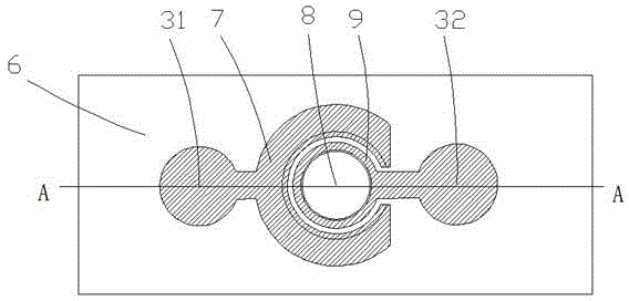
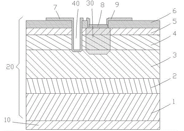
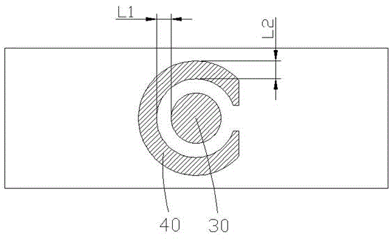
[0028] see Figure 1 to Figure 3 , the present invention provides a coplanar electrode analog photodetector chip, comprising: an epitaxial wafer 20 and an ohmic contact layer 10 formed on the back of the epitaxial wafer 20 . The epitaxial wafer 20 includes: a substrate 1, a buffer layer 2 formed on the substrate 1, an absorption layer 3 formed on the buffer layer 2, a transition layer 4 formed on the absorption layer 3, The top layer 5 formed on the transition layer 4, the passivation layer 6 formed on the top layer 5, the doped photosensitive region 30 formed in the absorption layer 3, the transition layer 4 and the top layer 5, formed on the The confinement groove 40 in the absorption layer 3, the transition layer 4, the top layer 5 and the passivation layer 6 is formed on the antireflection transition film layer 8 on the doped photosensit...


PUM


Abstract

The invention discloses a coplanar electrode analog photoelectric detector chip and a manufacturing method thereof. The coplanar electrode analog photoelectric detector chip comprises an epitaxial wafer and an ohm contact layer formed on the rear surface of the epitaxial wafer; the epitaxial wafer comprises a substrate, a buffer layer, an absorption layer, a transition layer, a top layer, a passivation layer, a doped photosensitive area, a limiting channel, an antireflective transition film layer, a P-type electrode metal layer and an N-type electrode metal layer; the top layer is a n-type III-V top layer with at least three elements; the doped photosensitive area is circular; the limiting channel is semi-circular and surrounds the doped photosensitive area. The manufacturing method of the coplanar electrode analog photoelectric detector chip is simple in process and high in finished product rate; the coplanar electrode analog photoelectric detector chip manufactured by the method has the characteristics of low distortion, low dark current, high linearity, high responsibility, high reliability and the like.

Description

technical field [0001] The invention relates to the technical field of optical communication, in particular to a coplanar electrode analog photodetector chip and a manufacturing method thereof. Background technique [0002] In general, photodetector chips can be divided into two categories: digital photodetector chips and analog photodetector chips. Analog photodetector chips are mainly used in fiber optic CATV (Community Antenna Television) receiving systems and fiber optic FTTP (Fiber To The Premise) receiving systems. Compared with conventional digital detector chips, the main feature of analog photodetector chips is that they require low combined second-order distortion and third-order intermodulation distortion, and require high linearity, high responsivity and low dark current. In order to achieve low distortion, the chip needs to be fully depleted at the lowest possible reverse bias voltage to ensure that the chip capacitance changes as little as possible with the in...

Claims


Application Information

Patent Timeline
IPC IPC(8): H01L31/11H01L31/0352H01L31/18
CPCH01L31/022408H01L31/11H01L31/184Y02P70/50
Inventor 王建
Owner SHENZHEN PHOGRAIN INTELLIGENT SENSING TECH CO LTD
Why Eureka
Try Eureka