LED package component, substrate and wafer level packaging method thereof
A technology of wafer-level packaging and LED packaging, which is applied in the direction of semiconductor devices, electrical components, circuits, etc., can solve the problems of wafer-level packaging that need to be studied, and achieve the effects of reducing packaging costs, simple operation process, and good heat dissipation performance
- Summary
- Abstract
- Description
- Claims
- Application Information
AI Technical Summary
Problems solved by technology
Method used
Image

Examples
Embodiment 1
[0033] Embodiment 1 (LED packaging device embodiment)
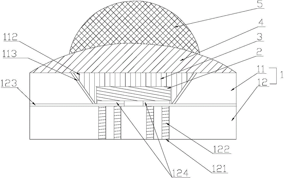
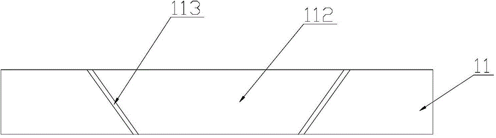
[0034] see figure 1 , a structural representation of the LED packaging device provided by the present invention picture . The LED packaging device provided by the present invention includes a substrate 1 , an LED chip 2 , a fluorescent layer 3 , a base lens 4 and a secondary lens 5 . Wherein, the substrate 1 is formed by assembling the first substrate 11 and the second substrate 12 . The first substrate 11 is provided with a through hole 112 (or called a pit), the side wall of the hole 112 has a certain slope and is an inclined surface, and the bottom opening of the hole 112 is smaller than the top opening of the hole. The longitudinal section of the hole 112 is trapezoidal. The size of the concave hole 112 is determined according to the size of the LED chip 2 , the larger the width of the concave hole 112 , the weaker the blocking effect of the sides on light, and the higher the light extraction efficiency. Howe...
Embodiment 2
[0040] Embodiment 2 (substrate embodiment)
[0041] see Image 6 ,Book invention A substrate 1 for LED chip wafer level packaging is provided. The substrate 1 is assembled from a first substrate 11 and a second substrate 12 .
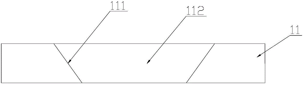
[0042] The first substrate 11 is provided with a through hole 112 (or called a pit), the side wall 111 of the hole 112 has a certain slope and is an inclined plane, and the bottom opening of the hole 112 is smaller than the top opening of the hole 112 , the longitudinal section of the concave hole 112 is trapezoidal. The size of the concave hole 112 is determined according to the size of the LED chip. The larger the width of the concave hole 112 is, the weaker the blocking effect of the sides on light is, and the higher the light extraction efficiency is. However, the width of the concave hole should also be controlled within a certain range to ensure that the substrate has a certain mechanical strength. Preferably in the present invention, the ...
Embodiment 3
[0046] Embodiment 3 (Wafer-level packaging method embodiment of LED packaging device)
[0047] The LED packaging device of embodiment 1 can be prepared by the following method, and its main steps are as follows:
[0048] 1) The making of the first substrate 11: see figure 2 ~3, prepare a silicon substrate 11, form a through hole 112 on the silicon substrate by chemical etching, and the side wall 111 of the hole 112 is an inclined plane, and the width of the opening at the bottom of the hole 112 is smaller than the width of the opening at the top of the hole 112; The depth of the concave hole 112 is about 200 μm (for example, 150-250 μm) higher than the thickness of the LED chip, so as to ensure good phosphor coating in the future. If the concave hole 112 is too deep, the thickness of the phosphor coating layer will increase, which is not conducive to light emission and heat dissipation; if the concave hole is too shallow, the phosphor concentration required to achieve whit...
PUM
 Abstract
Description
Claims
Application Information
 - R&D
- Intellectual Property
- Life Sciences
- Materials
- Tech Scout
- Unparalleled Data Quality
- Higher Quality Content
- 60% Fewer Hallucinations
Browse by: Latest US Patents, China's latest patents, Technical Efficacy Thesaurus, Application Domain, Technology Topic, Popular Technical Reports.
© 2025 PatSnap. All rights reserved.Legal|Privacy policy|Modern Slavery Act Transparency Statement|Sitemap|About US| Contact US: help@patsnap.com