OLED (organic light-emitting diode) packaging method and OLED packaging structure

A packaging method and packaging structure technology, which is applied in the manufacture of electrical components, electrical solid devices, semiconductor/solid devices, etc., can solve the problems of OLED device performance degradation, large molecular gap, and shortened lifespan, achieving good sealing effect and reducing oxygen Effect of water vapor and prolonging service life

Inactive Publication Date: 2015-04-29
TCL CHINA STAR OPTOELECTRONICS TECH CO LTD
View PDF8 Cites 10 Cited by
  • Summary
  • Abstract
  • Description
  • Claims
  • Application Information

AI Technical Summary

Problems solved by technology

However, the sealant used in UV glue packaging is an organic material, and its molecular gap is large after curing. The traditional OLED packaging method is adopted, because the sealant has curing defects, porosity, and weak bonding with the substrate and the packaging cover. For other reasons, water vapor and oxygen are more likely to penetrate into the internal sealing area through the gap, resulting in faster degradation of OLED device performance and shortened lifespan.

Method used


Image

  • OLED (organic light-emitting diode) packaging method and OLED packaging structure
  • OLED (organic light-emitting diode) packaging method and OLED packaging structure
  • OLED (organic light-emitting diode) packaging method and OLED packaging structure

Examples


Embodiment Construction

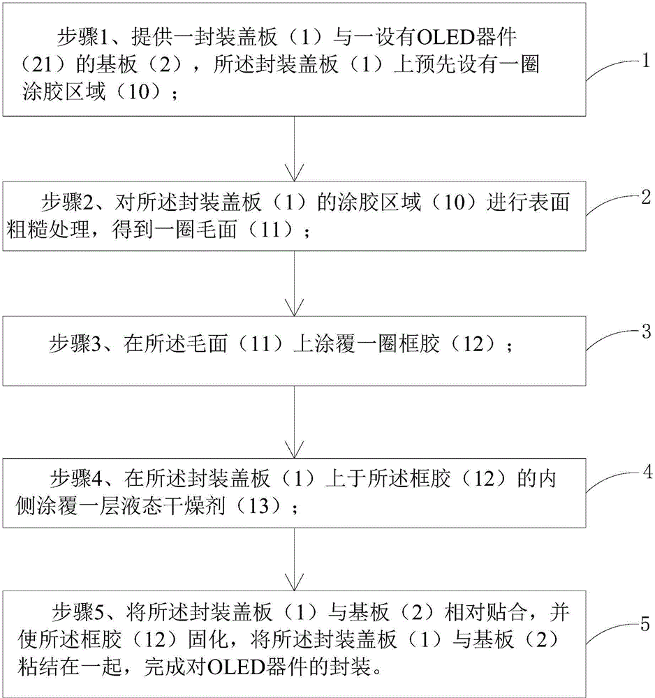
[0034] In order to further illustrate the technical means adopted by the present invention and its effects, the following describes in detail in conjunction with preferred embodiments of the present invention and accompanying drawings.

[0035] see figure 1 , the present invention provides a kind of OLED encapsulation method, comprises the following steps:

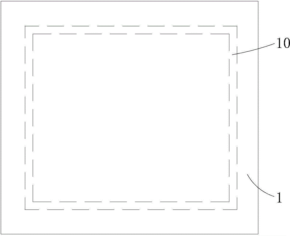
[0036] Step 1. Please also refer to figure 2 and Figure 7 , providing a packaging cover 1 and a substrate 2 , the packaging cover 1 is pre-set with a circle of glue-coating area 10 .

[0037] Both the packaging cover 1 and the substrate 2 are transparent substrates, preferably, the packaging cover 1 and the substrate 2 are both glass substrates. The substrate 2 is a substrate provided with an OLED device 21 , preferably, the substrate 2 is a TFT substrate provided with an OLED device 21 .

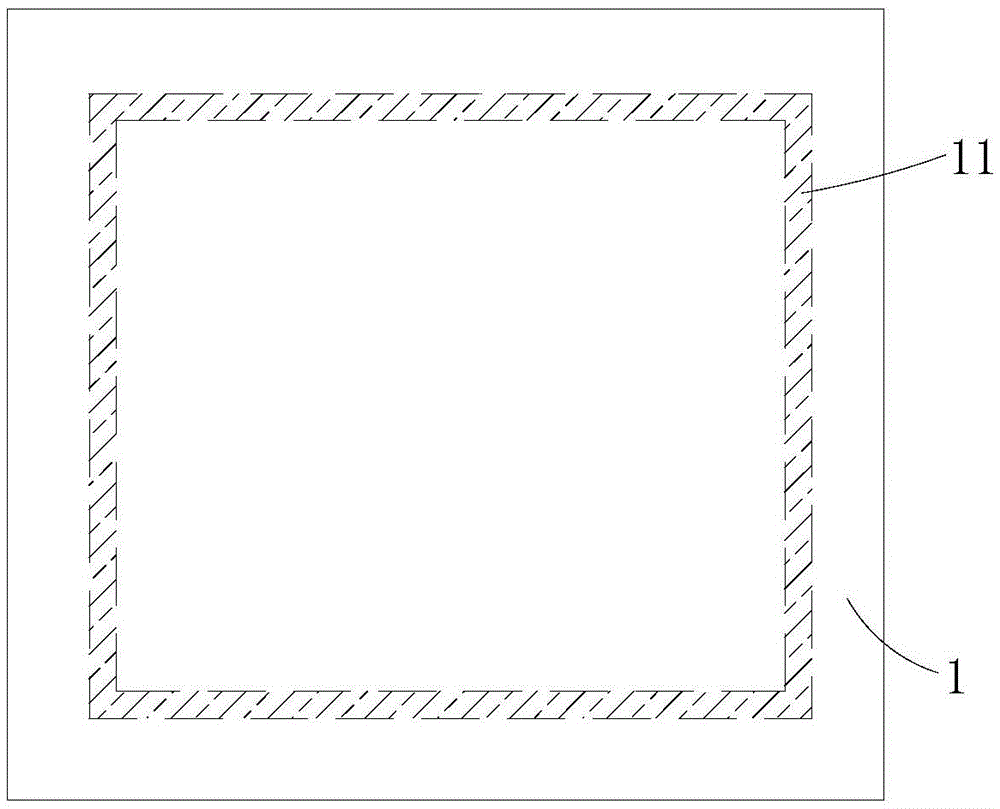
[0038] Step 2. Please also refer to image 3 and Figure 4 , roughening the surface of the glued area 10 of the package cover ...


PUM


Abstract

The invention provides an OLED (organic light-emitting diode) packaging method and an OLED packaging structure. The OLED packaging method comprises the following steps: step 1, providing a packaging cover plate (1) and a base plate (2) provided with an OLED device (21), wherein a circle of glued region (10) is pre-arranged on the packaging cover plate (1); step 2, performing surface roughening treatment on the glued region (10) of the packaging cover plate (1) to obtain a circle of rough surface; step 3, coating a circle of frame glue (12) on the rough surface (11); step 4, coating a layer of a liquid-state drying agent (13) on the inner side of the frame glue (12) on the packaging cover plate (1); step 5, relatively jointing the packaging cover plate (1) with the base plate (2) to cure the frame glue (12) and bonding the packaging cover plate (1) and the base plate (2) together to complete packaging of the OLED device. By adopting the method, the bonding force between the packaging cover plate and the base plate can be significantly packaged, and the sealing property is improved.

Description

technical field [0001] The invention relates to the field of display technology, in particular to an OLED packaging method and an OLED packaging structure. Background technique [0002] In the field of display technology, flat panel display technologies such as Liquid Crystal Display (LCD) and Organic Light Emitting Diode (OLED) have gradually replaced CRT displays. Among them, OLED has many advantages such as self-illumination, low driving voltage, high luminous efficiency, short response time, high definition and contrast, nearly 180° viewing angle, wide temperature range, flexible display and large-area full-color display, etc. It is widely used in mobile phone screens, computer monitors, full-color TVs, etc., and is recognized by the industry as the most promising display device. [0003] The OLED has an anode, an organic light emitting layer, and a cathode sequentially formed on a substrate. The biggest problem that restricts the development of the OLED industry and t...

Claims


Application Information

Patent Timeline
Patent Type & Authority Applications(China)
IPC IPC(8): H01L51/56H01L51/52
CPCH10K50/84H10K50/8426H10K50/846H10K71/00
Inventor 刘亚伟王宜凡
Owner TCL CHINA STAR OPTOELECTRONICS TECH CO LTD
Why Eureka
Try Eureka