Inverter of grid integrated driving circuit, grid integrated driver and driving method

A gate integrated drive and gate drive circuit technology, applied in instruments, static indicators, etc., can solve the problems of large DC loop, increased circuit noise, and large dynamic power consumption

Active Publication Date: 2015-05-06
王磊 +1
View PDF5 Cites 22 Cited by
  • Summary
  • Abstract
  • Description
  • Claims
  • Application Information

AI Technical Summary

Problems solved by technology

The traditional inverter is composed of a diode-connected transistor and a large-sized pull-down transistor. When the traditional inverter outputs a low level, there is a large DC loop, and due to the voltage drop on the pull-down transistor, the output of the inverter cannot minimum level reached
The clock-controlled inverter, which consists of a pull-down transistor and a clock-controlled pull-up transistor, will bring large dynamic power consumption due to the use of a clock signal, and when the clock signal goes low, the pull-up transistor will be completely turned off. At this time, for the circuit using oxide TFTs, the pull-down transistor still has a leakage current flowing. In order to keep the output of the inverter at a high level, a larger capacitor is required to maintain the voltage, which increases the circuit size. the area of
[0004] In the gate drive circuit, the more clock lines, the greater the load capacitance on the clock line, the higher the frequency, the greater the dynamic power consumption, and if the clock load differs greatly, it is easy to cause clock drift
Since the circuit maintains a low-level output time much longer than a high-level output time, multiple clocks will increase circuit noise and cause large fluctuations in the output voltage

Method used


Image

  • Inverter of grid integrated driving circuit, grid integrated driver and driving method
  • Inverter of grid integrated driving circuit, grid integrated driver and driving method
  • Inverter of grid integrated driving circuit, grid integrated driver and driving method

Examples


Embodiment 1

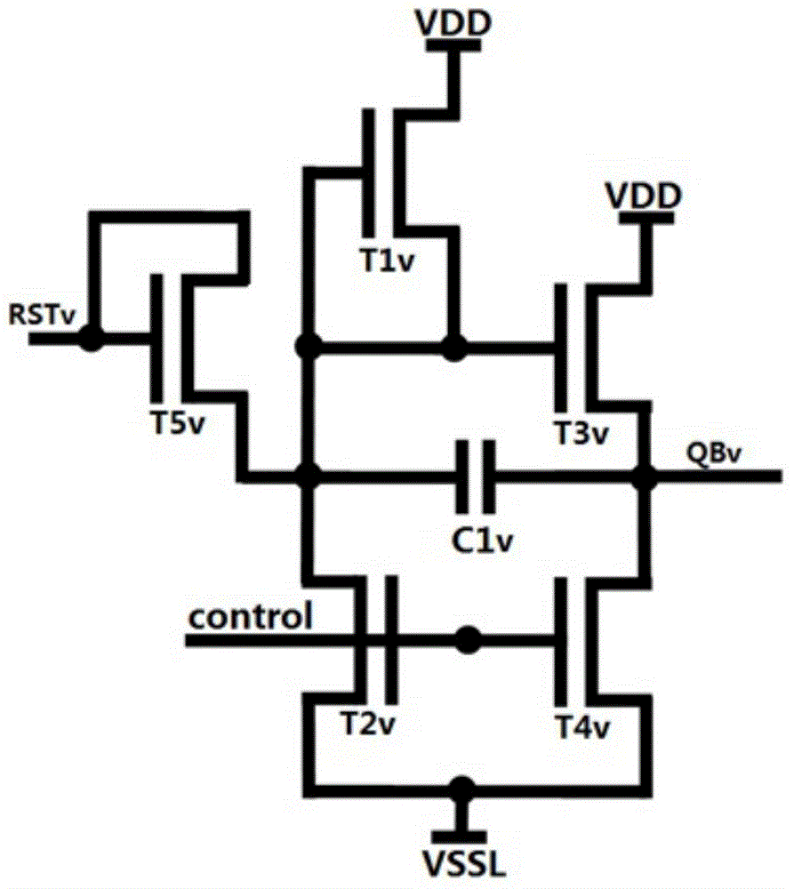
[0046] Such as figure 1 As shown, the inverter of the gate integrated drive circuit of this embodiment includes transistors T1v, T2v, T3v, T4v, T5v and coupling capacitor C1v, the drain of transistor T1v and the drain of T3v are connected to positive level VDD, The gate and source of the transistor T1v are connected to the drain of the transistor T2v, the gate of the transistor T3v, the source of the transistor T5v and one end of the capacitor C1v; the gate of the transistor T2v and the gate of the transistor T4v are connected to the control signal control, and the transistor T5v The gate and drain of the transistor are connected to the feedback signal RSTv, the source of the transistor T2v and the source of the transistor T4v are connected to the first negative level VSSL, and the drains of the transistors T3v and T4v are connected to the other end of the capacitor C1v to form an inverter output node QBv .

[0047] The transistors are all N-type depletion thin film transisto...

Embodiment 2

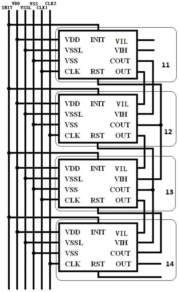
[0051] Such as figure 2 As shown, the gate integrated driver of this embodiment includes multi-level gate drive circuit units: a first-level gate drive circuit unit 11, a second-level gate drive circuit unit 12, and a third-level gate drive circuit unit 13 , the gate drive circuit unit 14 of the fourth stage, the gate drive circuit unit of each stage includes two input terminals VINH and VINL, three power supply terminals VDD, VSSL and VSS, wherein the voltage of VSSL is more negative than VSS, and a clock signal The input terminal CLK, the highest level of the clock signal is VDD, the lowest level is VSSL, two output terminals COUT and OUT, an initialization terminal INIT and a feedback terminal RST.

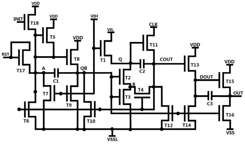
[0052] Such as image 3 As shown, each gate drive circuit unit includes transistors T1~T18 and coupling capacitors C1~C3, an input control signal VIH, an input signal VIL, a clock signal CLK, a feedback signal RST, an initialization signal INIT, the first The output signal C...

Embodiment 3

[0068] Compared with the embodiment 2, the integrated gate driving circuit of this embodiment removes the eighteenth transistor and omits the initialization process. Due to the new inverter module circuit used in the gate drive circuit, the QB point can automatically maintain a stable voltage slightly lower than VDD even if there is no initialization process. Therefore, the output signal of the circuit can still be maintained in the absence of input. stable low level.

[0069] Such as Figure 5 As shown, the integrated gate drive circuit of this embodiment includes multi-stage gate drive circuit units; the first output signal COUT of the gate drive circuit unit of this stage is used as the input control signal VIH and the upper gate drive circuit unit of the next stage. The feedback signal RST of the first-stage gate drive circuit unit, the second output signal OUT is used as the drive signal of the scanning line and the input signal VIL of the next-stage gate drive circuit u...


PUM


Abstract

The invention discloses an inverter of a grid integrated driving circuit. The inverter comprises transistors T1v-T5v and a coupling capacitor C1v, a second electrode of the T1v and a second electrode of the T3v are connected with positive level VDD, a grid and a first electrode of the T1v are connected with a second electrode of the T2v, a grid of the T3v, a first electrode of the T5v and one end of the C1v, a grid of the T2v and a grid of the T4v are connected with a control signal, the grid and a second electrode of the T5v are connected with a feedback signal RSTv, a first electrode of the T2v and a first electrode of the T4v are connected with first negative level, a second electrode of the T3v and a second electrode of the T4v are connected with the other end of the C1v, and an output node QBv of the inverter is formed. The invention further discloses the grid integrated driving circuit with the inverter and a driving method of the grid integrated driving circuit. The inverter is low in power consumption and noise and excellent in anti-jamming capability, and the output pull-up transistors and the inverter are rapid in action and can work under high frequency.

Description

technical field [0001] The invention relates to gate drive technology of flat panel displays, in particular to an inverter of a gate integrated drive circuit, a gate integrated driver and a driving method. Background technique [0002] In recent years, oxide thin film transistors have received great attention, which have the characteristics of high mobility, good consistency and stable electrical properties, and the preparation cost is low. Integrating the gate driving circuit on the display is beneficial to reduce the cost of the display device and realize the thin and light design of the display device with a narrow frame. However, only N-type oxide thin film transistors can be used in circuit design, and when the gate-source voltage is zero and the source-drain voltage is greater than zero, it cannot be completely turned off, and leakage current still flows. [0003] In the gate drive circuit, the module circuit that provides the control signal of the pull-down transisto...

Claims


Application Information

Patent Timeline
Patent Type & Authority Applications(China)
IPC IPC(8): G09G3/20
Inventor 吴为敬黄长煜姚若河
Owner 王磊
Why Eureka
Try Eureka