Piezoresistive pressure meter chip structure and preparation method thereof

A technology of chip structure and pressure gauge, which is applied in the direction of fluid pressure measurement, measuring force, and instrumentation by changing the ohmic resistance, can solve the problems of limiting the application of piezoresistive pressure sensors, the chip cannot be thinned, and the chip is small, so as to improve The effect of process yield, high penetration rate, and small total thickness

Inactive Publication Date: 2015-05-13
PEKING UNIV
View PDF5 Cites 2 Cited by
  • Summary
  • Abstract
  • Description
  • Claims
  • Application Information

AI Technical Summary

Problems solved by technology

The disadvantage of the above structure is that there is an inclination angle of 54.7 degrees between the side of the cavity and the strained silicon film, the size required at the bottom of the cavity is much larger than the strained silicon film, and the actual size of the chip cannot be very small due to the above problems; At the same time, the thickness of the chip is limited by the thickness of the silicon wafer and cannot be thinned to an ideal thickness, which limits the application of piezoresistive pressure sensors in some thickness-sensitive areas of the chip.

Method used


Image

  • Piezoresistive pressure meter chip structure and preparation method thereof
  • Piezoresistive pressure meter chip structure and preparation method thereof
  • Piezoresistive pressure meter chip structure and preparation method thereof

Examples


Embodiment Construction

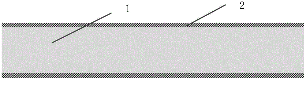
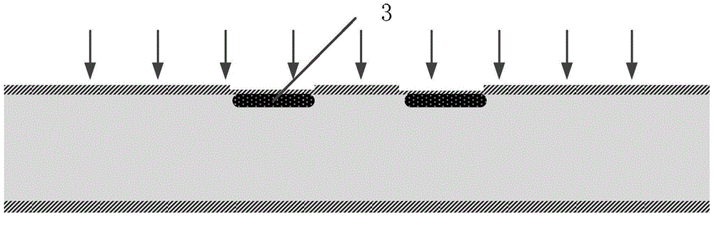
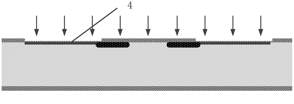
[0046] The present invention will be further described below through specific embodiments and accompanying drawings. As shown in Figure 1, the specific manufacturing process of the new piezoresistive pressure sensor chip structure using anodic bonding and silicon wafer thinning process is:

[0047] a) Preparation: the monocrystalline silicon substrate is used as the substrate 1 of the chip, the thickness of the substrate is 400 μm, there is silicon oxide 2 on the surface of the substrate, and the thickness of the silicon oxide is As shown in Figure 1(a);

[0048] b) The piezoresistor 3 and the heavily doped contact region 4 are manufactured on the silicon wafer by standard piezoresistive technology, as shown in Figure 1(b) and (c), including: photolithographic light boron region; Corrosion) SiO 2 Ion implantation B + ; boron advancement; lithographic boron-enriched region, RIE SiO 2 ; ion implantation B + ; boron propulsion;

[0049] c) Make lead holes (ie contact hol...


PUM

PropertyMeasurementUnit
thicknessaaaaaaaaaa

Abstract

The invention discloses a piezoresistive pressure meter chip structure and a preparation method thereof. The piezoresistive pressure meter chip structure comprises a pressure-sensitive resistor, a heavy doping contact area, a metal lead, a silicon strain film, a glass base, and a cavity formed between the silicon strain film and the glass base. According to the piezoresistive pressure meter chip structure, a pressure sensor of the structure has the advantages of being simple in process and small in chip size by being compared with the structure of the typical device; meanwhile, the anodic bonding and wafer grinding technologies are performed; the design processing method is compatible with the processing technology of the standard silicon piezoresistive pressure sensor; the device processing cost is low; the yield is high.

Description

technical field [0001] The invention belongs to the field of micro-electro-mechanical system (MEMS) sensor design, and relates to a MEMS piezoresistive pressure sensor and a method for manufacturing the pressure sensor on a single wafer by using a MEMS processing technique. Background technique [0002] MEMS (MicroElectroMechanical System) is a micro-electromechanical system, which is an emerging interdisciplinary high-tech research field. The piezoresistive pressure sensor based on MEMS technology is widely used in the modern market due to its excellent accuracy and reliability and relatively cheap manufacturing cost. Silicon-based piezoresistive pressure sensors have been widely used since the discovery of the piezoresistive properties of silicon materials in the mid-1950s. The working principle of the piezoresistive sensor is to fabricate four pressure-sensitive resistors in the stress concentration area by diffusion or ion implantation on a square or circular silicon st...

Claims


Application Information

Patent Timeline
Patent Type & Authority Applications(China)
IPC IPC(8): G01L9/04G01L1/22
Inventor 黄贤刘鹏张大成姜博岩王玮何军田大宇杨芳罗葵李婷张立
Owner PEKING UNIV
Why Eureka
Try Eureka