Miniature active matrix type organic light emitting display and manufacturing method thereof

A light-emitting display and matrix technology, applied in the field of miniature active-matrix organic light-emitting display and its production, can solve problems such as increased manufacturing difficulty, and achieve the effect of high reliability

Inactive Publication Date: 2014-09-17
NO 55 INST CHINA ELECTRONIC SCI & TECHNOLOGYGROUP CO LTD
View PDF7 Cites 15 Cited by
  • Summary
  • Abstract
  • Description
  • Claims
  • Application Information

AI Technical Summary

Problems solved by technology

[0005] The purpose of the present invention is to design a miniature active-matrix organic light-emitting display (i.e., miniature AMOLED display), while providing its fabrication method

Method used


Image

  • Miniature active matrix type organic light emitting display and manufacturing method thereof
  • Miniature active matrix type organic light emitting display and manufacturing method thereof
  • Miniature active matrix type organic light emitting display and manufacturing method thereof

Examples


Embodiment 1

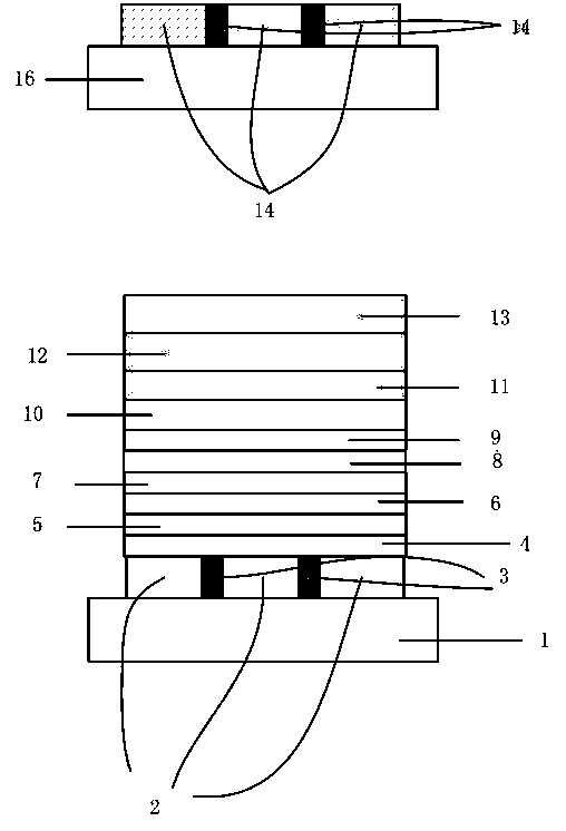
[0032] Such as Figure 4 shown.

[0033] A miniature active matrix organic light-emitting display, which mainly consists of a silicon wafer substrate 1, a pixel electrode 2, an insulating layer 3 (made of polyimide), a hole injection layer 4, a hole transport layer 5, a light-emitting layer 6, and an excitation layer. Sub barrier layer 7, electron transport layer 8, electron injection layer 9, cathode motor layer 10, sealing layer I11, sealing layer II12, sealing layer III13, color photoresist layer 14, black matrix layer 15 and glass substrate 16. A plurality of anode pixel electrodes 2 are made on the silicon substrate 1, and the material of the anode pixel electrodes 2 is a single-layer material or a multi-layer composite material, the single-layer material is Al, Mo or W, and the composite material is Mo / Al / Mo, Al / Mo, Cr / Al / Mo or Cr / Ti / Al / Mo, the total thickness of the anode pixel electrode 2 is between 60nm and 550nm, and the anode pixel electrode 15 is patterned to for...

Embodiment 2

[0035] Such as figure 1 , 3 shown.

[0036] A method for manufacturing a micro-active matrix organic light-emitting display includes manufacturing an anode pixel electrode on a silicon wafer substrate, manufacturing an OLED device layer on the anode electrode, manufacturing a thin film sealing layer for encapsulating an OLED structure, and manufacturing a color pixel electrode on a glass substrate. Fabrication of filter layer and black matrix, glue coating on silicon substrate and lamination with glass substrate. Specific steps are as follows:

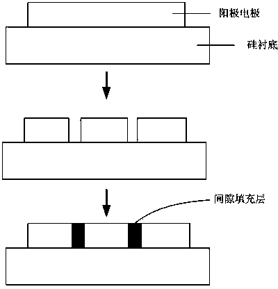
[0037] (1) Fabrication of anode pixel electrodes; the process is: silicon wafer substrate cleaning, deposition of anode electrodes by sputtering or electron beam evaporation, and patterning of anode pixel electrodes by dry etching, with a pixel area of ​​(3 μm to 5 μm )×(9μm~15μm). Such as figure 1 shown

[0038] The materials used for the anode pixel electrode are single-layer materials such as Al, Mo, W, etc., and also in...

example 1

[0047] The invention provides a preparation method for realizing a high-resolution color micro AMOLED display. An AMOLED display includes an anode, a cathode, and a light-emitting layer sandwiched in between. The resolution of the micro AMOLED display is determined by the pattern accuracy of the anode. The invention provides a feasible high-precision anode preparation scheme. refer to figure 1 , first deposit the anode film on the silicon substrate. The anode material is required to be electrically compatible with the silicon substrate and the OLED light-emitting layer. You can choose to use single-layer materials such as Al, Mo, W, or Mo / Al / Mo , Al / Mo, Cr / Al / Mo, Cr / Ti / Al / Mo and other multi-layer material structures, the total thickness of the electrode is between 60nm and 250nm.

[0048] Secondly, in order to achieve high patterning accuracy, plasma dry etching is chosen for patterning. Furthermore, methods such as laser etching can also be selected to realize anode patte...


PUM


Abstract

The invention provides a miniature active matrix type organic light emitting display and a manufacturing method of the miniature active matrix type organic light emitting display. The miniature active matrix type organic light emitting display is characterized by comprising a silicon substrate with a display driving circuit, and an OLED miniature full-color display device formed on the silicon substrate. The manufacturing method includes the steps of anode pixel electrode manufacture, OLED organic thin film evaporation, thin film sealing, manufacture of a color filter layer and a black matrix on cover plate glass, and attachment of the silicon substrate and the cover plate glass. By means of the miniature active matrix type organic light emitting display and the manufacturing method, the wet processing can be prevented from being generated in the preparation process of OLED devices, and performance of OLEDs can be ensured.

Description

technical field [0001] The invention relates to a display technology, in particular to an organic light emitting diode display technology, in particular to a miniature active matrix organic light emitting display and a manufacturing method thereof. Background technique [0002] An organic light emitting diode (OLED) display is a self-luminous display device that displays images by using light-emitting organic light-emitting diodes. Light is generated by controlling the energy produced when excitons fall back from an excited state. Excitons are generated by combining electrons and holes in the organic emissive layer. Generally, an OLED display includes a transistor driving matrix and an OLED display unit. [0003] Single crystal silicon is used as a substrate to make a transistor drive matrix, and since single crystal silicon has very high mobility, very high resolution can be achieved. The display size of organic light emitting diode displays fabricated using single cryst...

Claims


Application Information

Patent Timeline
Patent Type & Authority Applications(China)
IPC IPC(8): H01L27/32
Inventor 杨建兵杨洪宝李超
Owner NO 55 INST CHINA ELECTRONIC SCI & TECHNOLOGYGROUP CO LTD
Why Eureka
Try Eureka