

Preparation method of flexible super-hydrophobic and super-oleophobic structure
A super-hydrophobic, super-oleophobic, flexible technology, applied in the direction of microstructure technology, microstructure devices, manufacturing microstructure devices, etc., can solve the problems of difficult process, complicated process, and non-flexible structure, etc., and achieve low process cost , The process is simple and the effect of wide application value
- Summary
- Abstract
- Description
- Claims
- Application Information
AI Technical Summary
Problems solved by technology
Method used
Image

Examples
Embodiment 1
[0036] (1) Expose the underlying photoresist: Spin-coat a layer of SU-82000 photoresist on the substrate with a thickness of 5 μm, and expose without a mask;
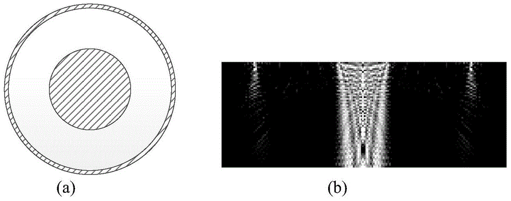
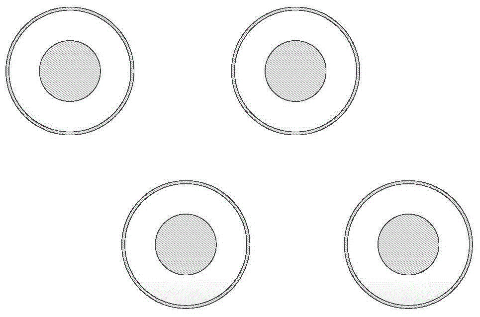
[0037] (2) The first exposure of the structural layer photoresist: spin-coat one deck of SU-82000 photoresist on the exposed SU-82000 photoresist in step (1), with a thickness of 10 μm for exposure; Such as image 3 The array pattern mask shown, wherein the diameter of the inner circle is 3 μm, the diameter of the outermost ring of the outer ring is 10 μm, the width of the ring is 0.5 μm, and the center-to-center distance between the array patterns is 15 μm;
[0038](3) The second exposure of the photoresist of the structural layer: use the mask of the light-transmitting circular array corresponding to step (2) for overlay exposure, and use a small exposure dose so that only the photoresist of the surface layer is 1 μm The cross-linking reaction will not be developed; the light-transmitting circle is consistent with th...
Embodiment 2
[0043] (1) Expose the underlying photoresist: spin-coat a layer of NR26-25000P on the substrate with a thickness of 10 μm, and expose without a mask;
[0044] (2) The first exposure of the structural layer photoresist: spin-coat one deck of SU-8GM 1070 on the exposed SU-8GM 1070 in step (1), the thickness is 12 μm, and expose; image 3 The array pattern mask shown, wherein the diameter of the inner circle is 6 μm, the diameter of the outer ring is 10 μm, the width of the ring is 0.8 μm, and the center-to-center distance between the array patterns is 30 μm;
[0045] (3) The second exposure of the photoresist of the structural layer: use the mask of the light-transmitting circular array corresponding to step (2) for overlay exposure, and use a small exposure dose so that only the photoresist of the surface layer is 1.5 μm The cross-linking reaction of the glue will not be developed; the light-transmitting circle is consistent with the distribution of the mask pattern used in ste...
Embodiment 3
[0050] (1) Expose the underlying photoresist: Spin-coat a layer of NR26-25000P photoresist on the substrate with a thickness of 20 μm, and expose without a mask;
[0051] (2) The first exposure of the photoresist of the structural layer: spin-coat one deck of NR26-25000P photoresist on the NR26-25000P photoresist after exposure in step (1), the thickness is 18 μm, and expose; Such as image 3 The array pattern mask shown, wherein the diameter of the inner circle is 9 μm, the diameter of the outer ring is 20 μm, the width of the ring is 1 μm, and the center-to-center distance between the array patterns is 42 μm;
[0052] (3) The second exposure of the photoresist of the structural layer: use the mask of the light-transmitting circular array corresponding to step (2) for overlay exposure, and use a small exposure dose so that only the photoresist of the surface layer is 2 μm The cross-linking reaction will not be developed; the light-transmitting circle is consistent with the d...
PUM
| Property | Measurement | Unit |
|---|---|---|
| Thickness | aaaaa | aaaaa |
| Thickness | aaaaa | aaaaa |
| Center distance | aaaaa | aaaaa |
Abstract
Description
Claims
Application Information