Supercharge Your Innovation With Domain-Expert AI Agents!

Transistor manufacturing method and transistor

A manufacturing method and transistor technology, applied in the fields of semiconductor/solid-state device manufacturing, semiconductor devices, electrical components, etc., can solve the problems of difficult alignment deviation control, high cost, multiple lithography layers, etc., to save chip area and reduce process. Cost, high alignment accuracy

Active Publication Date: 2017-11-24
FOUNDER MICROELECTRONICS INT
View PDF4 Cites 0 Cited by
  • Summary
  • Abstract
  • Description
  • Claims
  • Application Information

AI Technical Summary

Problems solved by technology

[0017] 1. There are many layers of photolithography: the production of the concentrated base region requires a separate photolithography layer process (step 2 above), and the process cost is relatively high;
[0018] 2. The width of the concentrated base region of the transistor must be greater than or equal to the width of the contact hole. In the above traditional method, the production of the concentrated base region and the contact hole is realized through different photoresist layers, and there must be a gap between different photoresist layers. There is a certain amount of alignment deviation. In order to ensure that the contact hole does not deviate from the area where the concentrated base region is located in the case of lithographic alignment deviation, it is necessary to make the width of the concentrated base region wider than the contact hole during chip design. Width is large enough (as in step 6 above Figure 7 d1 shown in ), this practice leads to larger chip area and higher cost
Because the photoresist layer in the concentrated base region is completed before the photoresist layer in the emission region, but because the photoresist layer in the concentrated base region is only implanted and doped in the preset area, it does not include the process steps for making step-shaped alignment marks. , so it is impossible to reserve and make alignment marks in the photoresist layer of the concentrated base area, that is to say, the photolithography of the emission area must be aligned with the alignment marks reserved in the photoresist layer of the active area to achieve alignment (with the photoresist layer of the concentrated base area Layers are not aligned and aligned)
[0020] Since the alignment deviation between layers of this indirect alignment is more difficult to control than that of direct alignment, in order to ensure that a safe distance is maintained between the emission region and the concentrated base region in the event of a large alignment deviation (to ensure that the two are not short-circuited), the set distance between the emission region and the concentrated base region must be sufficiently large during chip design, which leads to a larger chip area and higher cost

Method used


Image

  • Transistor manufacturing method and transistor
  • Transistor manufacturing method and transistor
  • Transistor manufacturing method and transistor

Examples


Embodiment Construction

[0042] In order to understand the above-mentioned purpose, features and advantages of the present invention more clearly, the present invention will be further described in detail below in conjunction with the accompanying drawings and specific embodiments. It should be noted that, in the case of no conflict, the embodiments of the present application and the features in the embodiments can be combined with each other.

[0043] In the following description, many specific details are set forth in order to fully understand the present invention, but the present invention can also be implemented in other ways different from those described here, therefore, the present invention is not limited to the specific embodiments disclosed below limit.

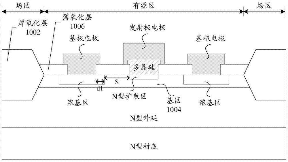
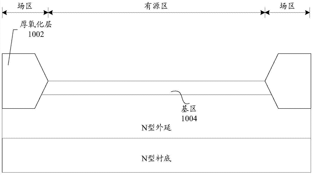
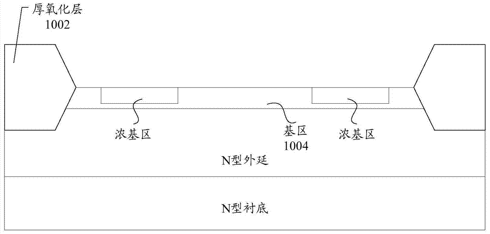
[0044] Figure 9 A flowchart of a method of manufacturing a transistor according to an embodiment of the present invention is shown.

[0045] Such as Figure 9 As shown, the transistor manufacturing method according to the embodiment of...


PUM


Abstract

The present invention provides a transistor manufacturing method and a transistor, wherein the transistor manufacturing method includes: growing a second oxide layer on the surface of the substrate on which the first oxide layer and the first base region are formed, the second oxide layer is located on the first above the base region; an emission region is formed in a first predetermined region on the second oxide layer; a contact hole is formed in a second predetermined region on the second oxide layer, wherein the second predetermined region is the same as the first predetermined region not intersecting; implanting doping elements into the surface layer of the first base region in the contact hole region; performing heat treatment on the substrate to activate the doping elements to form the second base region. The invention can skillfully integrate the photoresist layer of the concentrated base region and the photoresist layer of the contact hole, realize the self-alignment relationship between the photoresist layer of the concentrated base region and the photoresist layer of the contact hole, and solve the problem of the photoresist layer of the concentrated base region and the contact hole photoresist layer. Alignment misalignment of contact holes.

Description

technical field [0001] The invention relates to the technical field of semiconductor device manufacturing, in particular to a transistor manufacturing method and a transistor manufactured by the transistor manufacturing method. Background technique [0002] With the development of radio frequency and wireless communication technology, high frequency transistors are used more and more. High-frequency transistors in a broad sense include high-frequency bipolar transistors and high-frequency field-effect transistors. frequency bipolar transistor). [0003] The most important parameter to measure the performance of high-frequency transistors is its operating frequency. In order to increase the operating frequency of high-frequency transistors, a comb-like strip structure with small lines and a polysilicon emitter structure are used in practical processes. [0004] figure 1 It is a schematic cross-sectional structure diagram of a transistor. The transistor includes a collector...

Claims


Application Information

Patent Timeline
Patent Type & Authority Patents(China)
IPC IPC(8): H01L21/331H01L29/732H01L29/10
CPCH01L29/7322H01L21/2253H01L21/2257H01L21/283H01L21/31144H01L21/324H01L29/0804H01L29/1004H01L29/66272H01L29/732
Inventor 潘光燃文燕王焜石金成高振杰
Owner FOUNDER MICROELECTRONICS INT
Features
  • R&D
  • Intellectual Property
  • Life Sciences
  • Materials
  • Tech Scout
  • Unparalleled Data Quality
  • Higher Quality Content
  • 60% Fewer Hallucinations
Learn More