Dielectric isolation and junction isolation combined LIGBT (Lateral Insulated Gate Bipolar Transistor) device and manufacturing method

A technology of dielectric isolation and junction isolation, applied in the field of electronics, can solve the problems of the overall size of the device becoming larger, affecting the stability of the device, and the turn-off time becoming longer, so as to reduce the turn-off time, suppress the negative resistance effect and the negative resistance effect. the effect of elimination

Inactive Publication Date: 2015-05-20
NANJING UNIV OF POSTS & TELECOMM
View PDF4 Cites 12 Cited by
  • Summary
  • Abstract
  • Description
  • Claims
  • Application Information

AI Technical Summary

Problems solved by technology

The difference from LDMOS is that LIGBT is a bipolar device. When it is turned on, there is not only electron current, but the anode P+ will inject holes into the drift region to generate electron current, which makes the turn-off time longer.
Generally, the anode short-circuit structure that reduces the turn-off time can provide an electron extraction channel when the device is turned off, but there is a process of transition from LDMOS mode to LIGBT mode when th

Method used


Image

  • Dielectric isolation and junction isolation combined LIGBT (Lateral Insulated Gate Bipolar Transistor) device and manufacturing method
  • Dielectric isolation and junction isolation combined LIGBT (Lateral Insulated Gate Bipolar Transistor) device and manufacturing method
  • Dielectric isolation and junction isolation combined LIGBT (Lateral Insulated Gate Bipolar Transistor) device and manufacturing method

Examples


Embodiment Construction

[0023] Specific embodiments of the present invention will be further described in detail below.

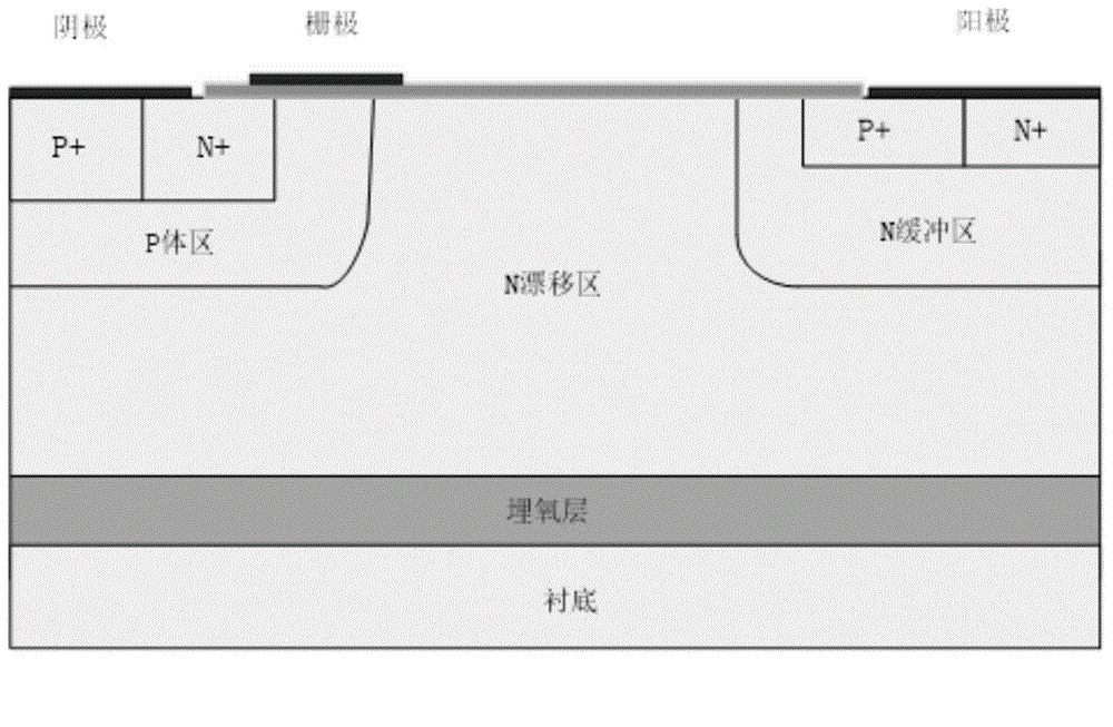
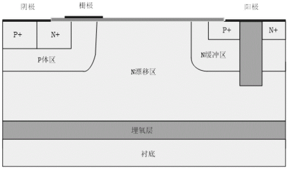
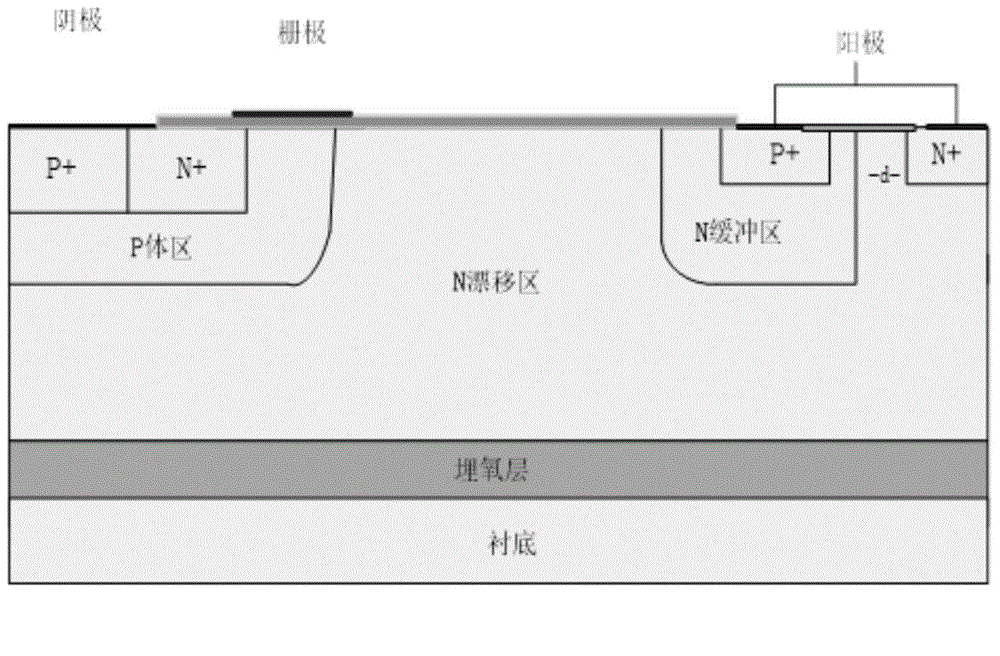
[0024] as attached Figure 4 As shown, the LIGBT device based on the combination of dielectric isolation and junction isolation has a buried oxide layer 2 on a silicon substrate 1; a drift region 3 is located on the buried oxide layer; one side of the drift region is a cathode region, and the other side is an anode region; In the P body region 4, there are cathode heavily doped P+ region 5 and cathode heavily doped N+ region 6; lightly doped N buffer region 7 under the anode P+ region 8, lightly doped P buffer region under the anode heavily doped N+ region 11 The region 10 and the P buffer region 10 do not completely surround the anode heavily doped N+ region 11, and the gap distance is d, which is adjustable. The anode P+ region 8 and the N+ region 11 are separated by a silicon dioxide dielectric 9; the upper part of the device is the cathode 12, the gate 13, and the anode 15; t...


PUM


Abstract

The invention relates to a dielectric isolation and junction isolation combined LIGBT (Lateral Insulated Gate Bipolar Transistor) device and a manufacturing method and belongs to the technical field of electronics. According to the LIGBT device, for an anode area of the traditional short-circuit LIGBT, a dielectric isolation and junction isolation combined structure is adopted, dielectric isolation is adopted between N+ and P+ of an anode, and junction isolation is adopted below N+. According to the novel dielectric isolation and junction isolation combined structure, on one hand, on the basis that shorter off time of the device is guaranteed, during conduction, the negative resistance effect of the negative resistance effect can be eliminated and the performance and the stability of the device are improved, and on the other hand, the size area of the device can also be reduced.

Description

technical field [0001] The invention relates to a LIGBT device combined with dielectric isolation and junction isolation and a manufacturing method, belonging to the field of electronic technology. Background technique [0002] Lateral Insulator Gate Bipolar Transistor LIGBT (Lateral Insulator Gate Bipolar Transistor) is a composite power device combined with a MOS gate device structure and a bipolar transistor structure. It has the characteristics of high input impedance and low conduction voltage drop. The difference from LDMOS is that LIGBT is a bipolar device. When it is turned on, there is not only electron current, but the anode P+ will inject holes into the drift region to generate electron current, which makes the turn-off time longer. Generally, the anode short-circuit structure that reduces the turn-off time can provide an electron extraction channel when the device is turned off, but there is a process of transition from LDMOS mode to LIGBT mode when the device is...

Claims


Application Information

Patent Timeline
IPC IPC(8): H01L29/739H01L29/06H01L21/331
Inventor 刘雪松成建兵俞露露陈旭东郭厚东滕国兵
Owner NANJING UNIV OF POSTS & TELECOMM
Why Eureka
Try Eureka