Preparation method of crystalline silicon solar battery multi-layer antireflection film
An anti-reflection film, solar cell technology, applied in circuits, photovoltaic power generation, electrical components and other directions, can solve the problems of high cost, poor anti-PID performance, reduced production cost, etc., to reduce production costs, good anti-PID performance, comprehensive good performance
- Summary
- Abstract
- Description
- Claims
- Application Information
AI Technical Summary
Problems solved by technology
Method used
Image
Examples
Embodiment 1
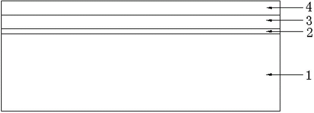
[0013] Embodiment 1: as attached figure 1 As shown, a method for preparing a multilayer anti-reflection film for a crystalline silicon solar cell, a P-type polysilicon wafer 1 of 156*156 cm is placed in a coating machine after completing the processes of acid texturing, phosphorus diffusion, and etching and cleaning. When making the anti-reflection film layer, first make a layer of SiO on the surface of the solar cell silicon wafer 1 2 Coating I2, then SiO 2 Make a layer of SiO on the surface of the film layer Ⅰ2 2 Layer II3, finally on SiO 2 The SiNx anti-reflection coating layer 4 is fabricated on the surface of the coating layer II3, and the specific steps are as follows:
[0014] (1) Pre-cleaning: use N 2 as diluent gas, N 2 The flow range is 3slm, the graphite boat enters the PECVD equipment, and then utilizes NH 3 For pre-cleaning, NH 3 The flow rate is 5slm, the pre-cleaning time is 1200s, the pressure in the tube is 2000mtorr, the RF power is 5500W, and the duty...
Embodiment 2
[0018] Embodiment 2: Another method for preparing a multilayer anti-reflection film for a crystalline silicon solar cell, the specific steps are as follows:
[0019] (1) Pre-cleaning: use N 2 as diluent gas, N 2 The flow range is 5slm, the graphite boat enters the PECVD equipment, and then utilizes NH 3 For pre-cleaning, NH 3 The flow rate is 5slm, the pre-cleaning time is 150s, the pressure inside the tube is 1800mtorr, the RF power is 5000W, and the duty cycle is 1 / 5ms;
[0020] (2) Making the first layer of SiO 2 Film layer Ⅰ: the first layer of SiO is plated after pre-cleaning 2 Membrane Ⅰ2, through the oxidizing gas N 2 Oxidation reaction in 0 to PECVD furnace to generate SiO 2 Coating I2, the N 2 0 flow rate is 7000, the SiO 2 The thickness of film layer I2 is 10nm;
[0021] (3) Making the second layer of SiO 2 Film layer Ⅱ: in the first layer of SiO 2 The second layer of SiO is plated on the film layer Ⅰ2 2 Membrane II (3), through the oxidizing gas N 2 Oxi...
Embodiment 3
[0023] Embodiment 3: Another kind of preparation method of multilayer anti-reflection film of crystalline silicon solar cell, concrete steps are as follows:
[0024] (1) Pre-cleaning: use N 2 as diluent gas, N 2 The flow range is 1slm, the graphite boat enters the PECVD equipment, and then utilizes NH 3 For pre-cleaning, NH 3 The flow rate is 8slm, the pre-cleaning time is 100s, the pressure in the tube is 2500mtorr, the RF power is 6000W, and the duty cycle is 1 / 8ms;
[0025] (2) Making the first layer of SiO 2 Film layer Ⅰ: the first layer of SiO is plated after pre-cleaning 2 Membrane Ⅰ2, through the oxidizing gas N 2 Oxidation reaction in 0 to PECVD furnace to generate SiO2 Coating I2, the N 2 0 flow rate is 7500, the SiO 2 The thickness of film layer Ⅰ2 is 8nm;
[0026] (3) Making the second layer of SiO 2 Film layer Ⅱ: in the first layer of SiO 2 The second layer of SiO is plated on the film layer Ⅰ2 2 Membrane II (3), through the oxidizing gas N 2 Oxidation ...
PUM
| Property | Measurement | Unit |
|---|---|---|
| Thickness | aaaaa | aaaaa |
| Thickness | aaaaa | aaaaa |
| Thickness | aaaaa | aaaaa |
Abstract
Description
Claims
Application Information
