Amorphous zinc oxide-based thin film transistor and preparation method thereof

A thin-film transistor, zinc oxide-based technology, applied in the direction of transistors, semiconductor/solid-state device manufacturing, semiconductor devices, etc., can solve the problems of high manufacturing cost, scarce content, and non-environmental protection, achieve uniform distribution, simple steps, and reduce industrial manufacturing cost effect

Inactive Publication Date: 2015-06-03
PEKING UNIV
View PDF3 Cites 13 Cited by
  • Summary
  • Abstract
  • Description
  • Claims
  • Application Information

AI Technical Summary

Problems solved by technology

However, because In in the material is a rare element, the content in the earth is rare, and In and Ga elements are poisonous, the manufacturing cost is high and it is not environmentally friendly.

Method used


Image

  • Amorphous zinc oxide-based thin film transistor and preparation method thereof
  • Amorphous zinc oxide-based thin film transistor and preparation method thereof
  • Amorphous zinc oxide-based thin film transistor and preparation method thereof

Examples


Embodiment Construction

[0032] The present invention will be further described through the embodiments below in conjunction with the accompanying drawings.

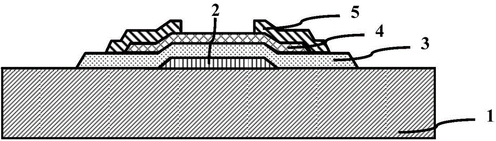
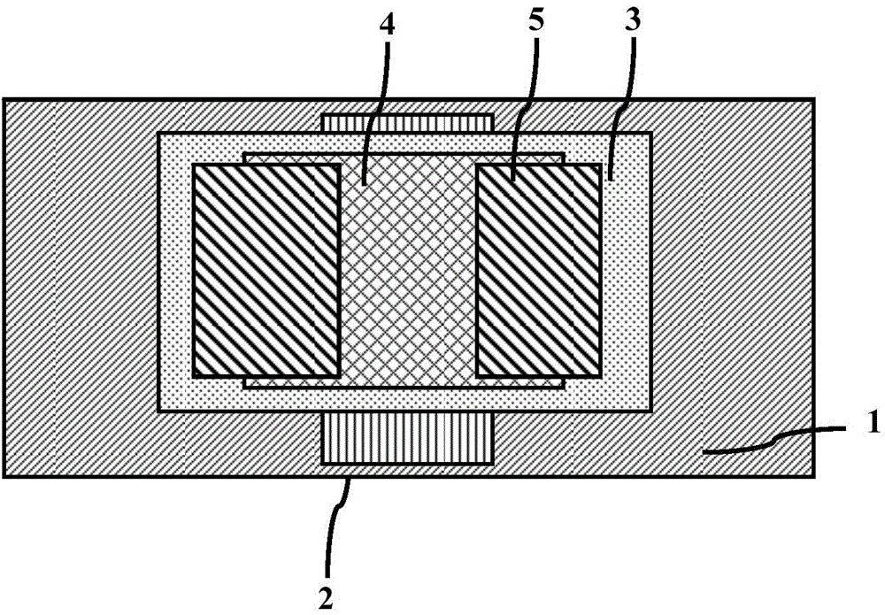
[0033] Such as figure 1 and figure 2 As shown, the amorphous zinc oxide-based thin film transistor of the present invention includes: a substrate 1, a gate electrode 2, a gate dielectric layer 3, a channel layer 4, a source electrode and a drain electrode 5, wherein the gate electrode is formed on the substrate 1 2. Form a gate dielectric layer 3 on the gate electrode 2 , form a channel layer 4 on the gate dielectric layer 3 , and form a source electrode and a drain electrode 5 at both ends of the channel layer 4 .

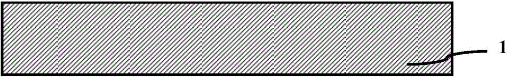
[0034] An embodiment of the preparation method of the thin film transistor of the present invention is shown in Figure 3 (a) to (e), including the following steps:

[0035] 1) Use transparent glass or plastic as the substrate 1, as shown in Figure 3(a), grow a conductive film of ITO with a thickness of 50 to 150 nanometers on the...


PUM

PropertyMeasurementUnit
particle sizeaaaaaaaaaa
sizeaaaaaaaaaa
surface roughnessaaaaaaaaaa

Abstract

The invention discloses an amorphous zinc oxide-based thin film transistor and a preparation method thereof. The amorphous zinc oxide-based thin film transistor comprises a substrate, a grid electrode, a grid medium layer, a channel layer, a source electrode and a drain electrode, wherein the channel layer is made of a zinc oxide semiconductor material doped with aluminum and tin, the content of aluminum oxide is 3-9% (in mass), and the content of tin oxide is 3-50% (in mass). The grain size of a prepared ATZO (ZnO+Al2O3+SnO2) semiconductor thin film is about 10nm, the distribution is uniform, and the prepared ATZO semiconductor thin film is a nanometer crystal oxide semiconductor. The preparation method has the advantages that the steps are simple, the manufacturing cost is low, the uniformity is good, the method is applied to low-temperature technology, the positive effect on improving the property of the thin film transistor device is improved, the properties, such as migration rate, switch ratio, threshold voltage and sub-threshold swinging rate, of the device, are improved, the method is suitable for transparent display and flexible display techniques, and the like.

Description

technical field [0001] The invention belongs to the field of semiconductor industry and flat panel display, and in particular relates to an amorphous zinc oxide-based thin film transistor and a preparation method thereof. Background technique [0002] With the gradual development of the information age, information display technology is becoming more and more mature. In the field of display technology, flat panel display technology (such as liquid crystal display LCD) has replaced the traditional bulky and high energy-consuming cathode ray tube display and has occupied a mainstream position in the display field. [0003] Early LCD flat panel display generally adopts a passive form, but its display response speed is slow and the contrast ratio is low, so it is only suitable for occasions where the display quality is not high; for the mainstream application fields that require high-performance display requirements, including mobile phones, TVs, etc. , computers, etc., which a...

Claims


Application Information

Patent Timeline
Patent Type & Authority Applications(China)
IPC IPC(8): H01L29/786H01L21/34
CPCH01L29/786H01L29/1033H01L29/66742H01L29/78693
Inventor 韩德栋丛瑛瑛黄福青单东方张索明田宇王漪张盛东刘晓彦康晋锋
Owner PEKING UNIV
Why Eureka
Try Eureka