Method for preparing thin-film transistor on flexible substrate

A technology of thin film transistors and conductive films, which is applied in the field of flat panel display, can solve the problems of high preparation cost, difficulty in application, and scarce content, and achieve the effects of low preparation cost, low production cost and improved performance

Inactive Publication Date: 2014-01-15
BOE TECH GRP CO LTD
View PDF5 Cites 5 Cited by
  • Summary
  • Abstract
  • Description
  • Claims
  • Application Information

AI Technical Summary

Problems solved by technology

Among them, IGZO is currently the most promising transparent semiconductor material. However, because indium in the material is a rare element, the content in the earth is rare and toxic, the preparation cost is high and it is not environmentally friendly, so it is difficult to apply in large-scale production.

Method used


Image

  • Method for preparing thin-film transistor on flexible substrate
  • Method for preparing thin-film transistor on flexible substrate
  • Method for preparing thin-film transistor on flexible substrate

Examples


Embodiment Construction

[0032] The present invention will be further elaborated below through specific embodiments in conjunction with the accompanying drawings.

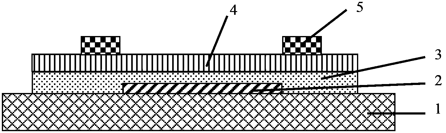
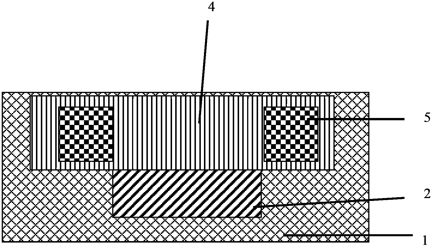
[0033] Such as figure 1 and figure 2 As shown, the thin film transistor of the present invention includes: a substrate 1, a gate electrode 2, a gate dielectric layer 3, a channel layer 4, a source electrode and a drain electrode 5, wherein the gate electrode 2 is formed on the substrate 1, and the gate electrode A gate dielectric layer 3 is formed on the gate dielectric layer 2, a channel layer 4 is formed on the gate dielectric layer 3, and a source electrode and a drain electrode 5 are respectively formed at both ends of the channel layer 4.

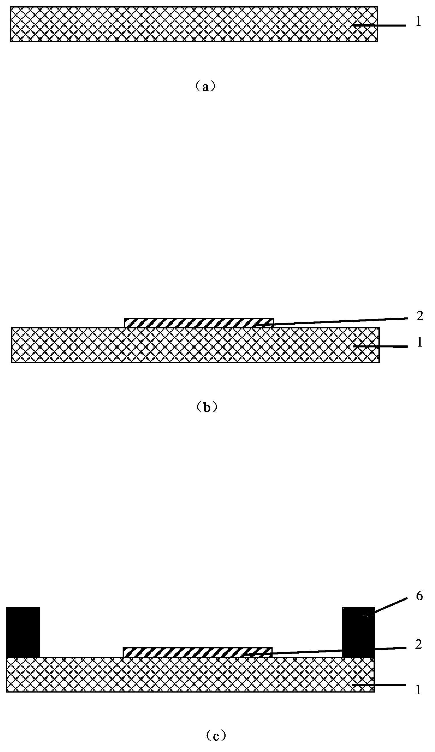
[0034] One embodiment of the preparation method of the thin film transistor of the present invention consists of image 3 (a) to (e), including the following steps:

[0035] 1) Using flexible plastic as the substrate 1, such as image 3 As shown in (a), a conductive thin film of ITO with a thi...


PUM

PropertyMeasurementUnit
thicknessaaaaaaaaaa
thicknessaaaaaaaaaa
thicknessaaaaaaaaaa

Abstract

The invention discloses a method for preparing a thin-film transistor on a flexible substrate. According to the invention, a thin-film transistor is prepared on a flexible plastic substrate. An aluminum-doped zinc oxide semiconductor material is used for forming a transparent conductive semiconductor channel layer. During the preparation process, an appropriate amount of oxygen is added by using the unique technology and thus the aluminum-doped zinc oxide presents a semiconductor characteristic and exhibits a high migration characteristic, thereby effectively improving the performance of the thin-film transistor. Meanwhile, the zinc oxide aluminum film is an environment-friendly material and the process is simple, so that the application prospect is wide. Moreover, the preparation method of simultaneous preparation of an insulated gate dielectric layer and a semiconductor channel layer is employed, thereby simplifying the preparation process. And an interface state of films on the flexible substrate can be effectively improved; the device performance is improved; the manufacturing cost is lowered; and the large-scale production can be realized.

Description

technical field [0001] The invention belongs to the field of flat panel display, and in particular relates to a preparation method of a thin film transistor on a flexible substrate. Background technique [0002] Flexible display technology is a hot topic in the display field in recent years. The research and application of flexible display has attracted extensive attention in the field of display at home and abroad. A new type of display technology is quietly rising, which will revolutionize the display industry. Flexible display is generally considered to be the next generation of new displays, and it will have very broad application prospects and huge commercial potential in many aspects such as electronic paper, electronic maps, large-scale advertisements, mobile phones, computers, and national defense and military affairs. Whether it is the cathode ray display CRT (Cathode Ray Tude) used in the early days, or the current mainstream liquid crystal display LCD (Liquid Cr...

Claims


Application Information

Patent Timeline
Patent Type & Authority Applications(China)
IPC IPC(8): H01L21/336
CPCH01L29/7869H01L21/02521H01L21/02631H01L29/227
Inventor 韩德栋王薇蔡剑王亮亮耿友峰刘力锋王漪张盛东刘晓彦康晋锋
Owner BOE TECH GRP CO LTD
Why Eureka
Try Eureka