Method for forming high-frequency IC wire and inductive coil pack

A technology of inductance coils and wires, which is applied in the direction of electrical components, semiconductor/solid-state device manufacturing, circuits, etc., and can solve problems such as process defects, wires cannot provide current carrying function, and limit the application of copper metal.

Inactive Publication Date: 2004-03-24
GRACE SEMICON MFG CORP
View PDF0 Cites 0 Cited by
  • Summary
  • Abstract
  • Description
  • Claims
  • Application Information

AI Technical Summary

Problems solved by technology

[0002] In the semiconductor manufacturing process, it is necessary to rely on metal wires to connect each transistor (interconnection) to play the function of the semiconductor device. Since the semiconductor components, chip manufacturers have used aluminum as the main wire material because of its small resistance value and circuit resistance. The deposition and etching of patterns are very easy, but when the semiconductor manufacturing process goes deep into sub-micron, the density of components becomes higher and higher, and the wires become relatively thinner. On the other hand, the requirements of low power consumption and high-speed IC Aluminum conductors cannot provide reliable current carrying function
[0003] How to reduce the resistance of the connection is very important, because the components with small resistance will consume less power, the RC delay time will be shorter, and the speed of IC components will be faster, so there are copper wires, due to the resistance of copper The value is smaller than that of aluminum; although copper has a lower resistance value than aluminum, the diffusion rate of copper in silicon is very high, resulting in reduced reliability of components due to copper contamination of the silicon substrate, and copper wires cannot be etched to form wires Therefore, after semiconductors en...

Method used


Image

  • Method for forming high-frequency IC wire and inductive coil pack
  • Method for forming high-frequency IC wire and inductive coil pack
  • Method for forming high-frequency IC wire and inductive coil pack

Examples


Embodiment Construction

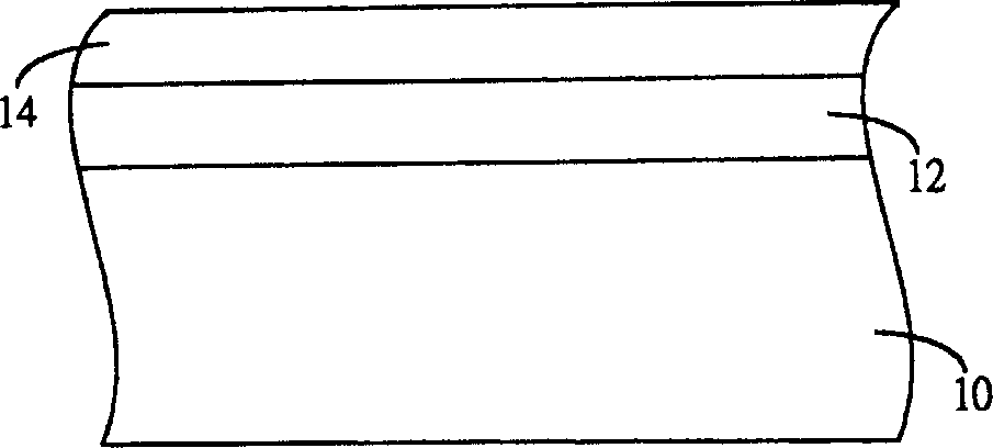
[0012] see Figure 2A First, a substrate 10 is provided, and a component layer 12 is formed on the substrate 10. The component layer 12 is different depending on different semiconductor structures. The component layer 12 includes active regions, isolation structures and passive components, etc., such as in gold In an oxygen-semiconductor field-effect transistor (MOSFET), the component layer 12 can be a gate oxide layer, a gate stack structure of a polysilicon layer, and source / drain structures; Resist 14, the photoresist 14 formed here is a negative photoresist, that is, the exposed part will become cross-linked and polymerized due to photochemical reaction, and harden after development. Remains on the surface of the substrate, the unexposed part is dissolved by the developer.

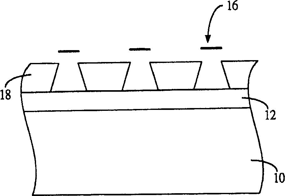
[0013] see next Figure 2B A masking layer 16 is covered on the photoresist 14, and after the alignment and exposure steps, a postexposure bake (postexposure bake) of ammonia gas is performed to redu...


PUM


Abstract

This invention discloses a method for forming high frequency IC wire and inductance coil components which is to form patternized photoresistance on a base surface after finishing processing all components on it then to form a copper thin film on the base and photoresistance utilizing a physical deposition method. Since the copper films are not connected, good copper wire structure is formed on the component zone of the base surface after photoresistance floatation to guarantee complete on-line structure among semicaonductor components.

Description

【Technical field】 [0001] The invention relates to a manufacturing method of a semiconductor component, in particular to a method of using copper material to form connecting wires between components. 【Background technique】 [0002] In the semiconductor manufacturing process, it is necessary to rely on metal wires to connect each transistor (interconnection) to play the function of the semiconductor device. Since the semiconductor components, chip manufacturers have used aluminum as the main wire material because of its small resistance value and circuit resistance. The deposition and etching of patterns are very easy, but when the semiconductor manufacturing process goes deep into sub-micron, the density of components becomes higher and higher, and the wires become relatively thinner. On the other hand, the requirements of low power consumption and high-speed IC Aluminum conductors cannot provide a reliable current carrying function. [0003] How to reduce the resistance of ...

Claims


Application Information

Patent Timeline
IPC IPC(8): H01L21/70
Inventor 高荣正
Owner GRACE SEMICON MFG CORP
Why Eureka
Try Eureka