Time delay-based double-track pre-charge logic NAND gate circuit and Time delay-based double-track pre-charge logic exclusive or gate circuit

A technology of NOT gate circuit and logical difference, applied in the direction of logic circuit with logic function, etc., can solve the problem of unbalanced circuit power consumption, and achieve the effect of solving the problem of charge sharing

Inactive Publication Date: 2015-06-03
PEKING UNIV
View PDF3 Cites 10 Cited by
  • Summary
  • Abstract
  • Description
  • Claims
  • Application Information

AI Technical Summary

Problems solved by technology

[0013] However, such a circuit still has certain problems that lead to unbalanced power consumption. Figure 1e Take the NAND gate precharge stage of the circuit shown as an example to simulate, and the waveform diagram is as follows Figure 1k shown
It can be seen from the figure that the upper jump edge of the dual-rail signal input of the ...

Method used


Image

  • Time delay-based double-track pre-charge logic NAND gate circuit and Time delay-based double-track pre-charge logic exclusive or gate circuit
  • Time delay-based double-track pre-charge logic NAND gate circuit and Time delay-based double-track pre-charge logic exclusive or gate circuit
  • Time delay-based double-track pre-charge logic NAND gate circuit and Time delay-based double-track pre-charge logic exclusive or gate circuit

Examples


Embodiment Construction

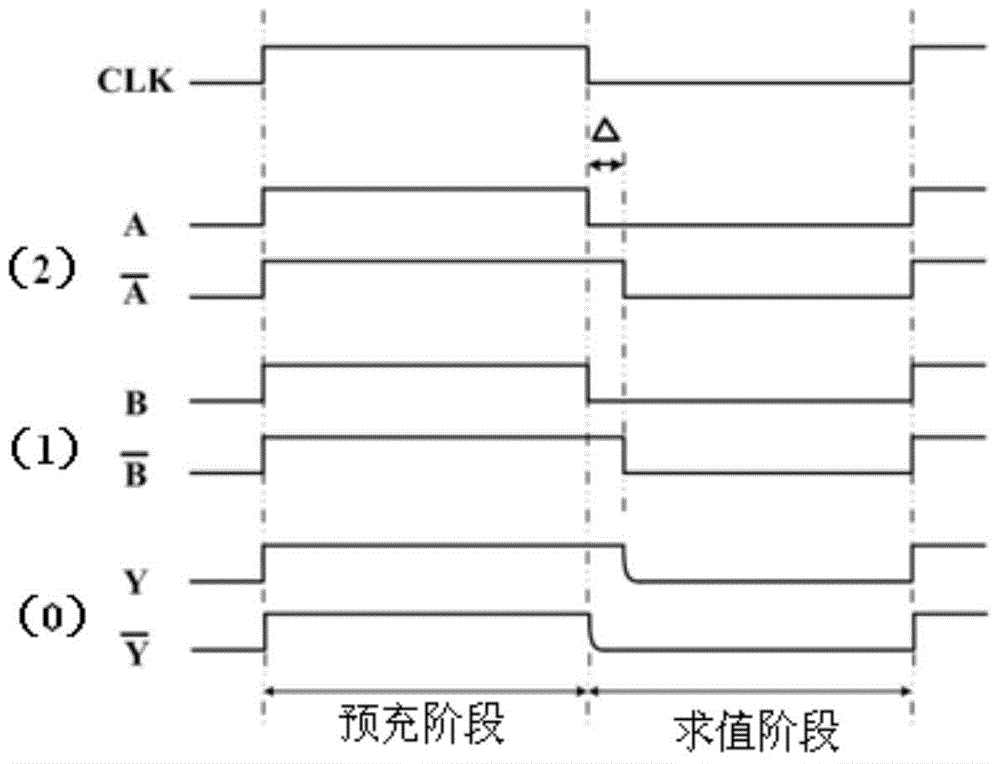
[0050] The present invention will be described in further detail below in conjunction with the accompanying drawings and embodiments. The following examples are used to illustrate the present invention, but should not be used to limit the scope of the present invention.

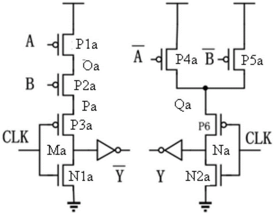
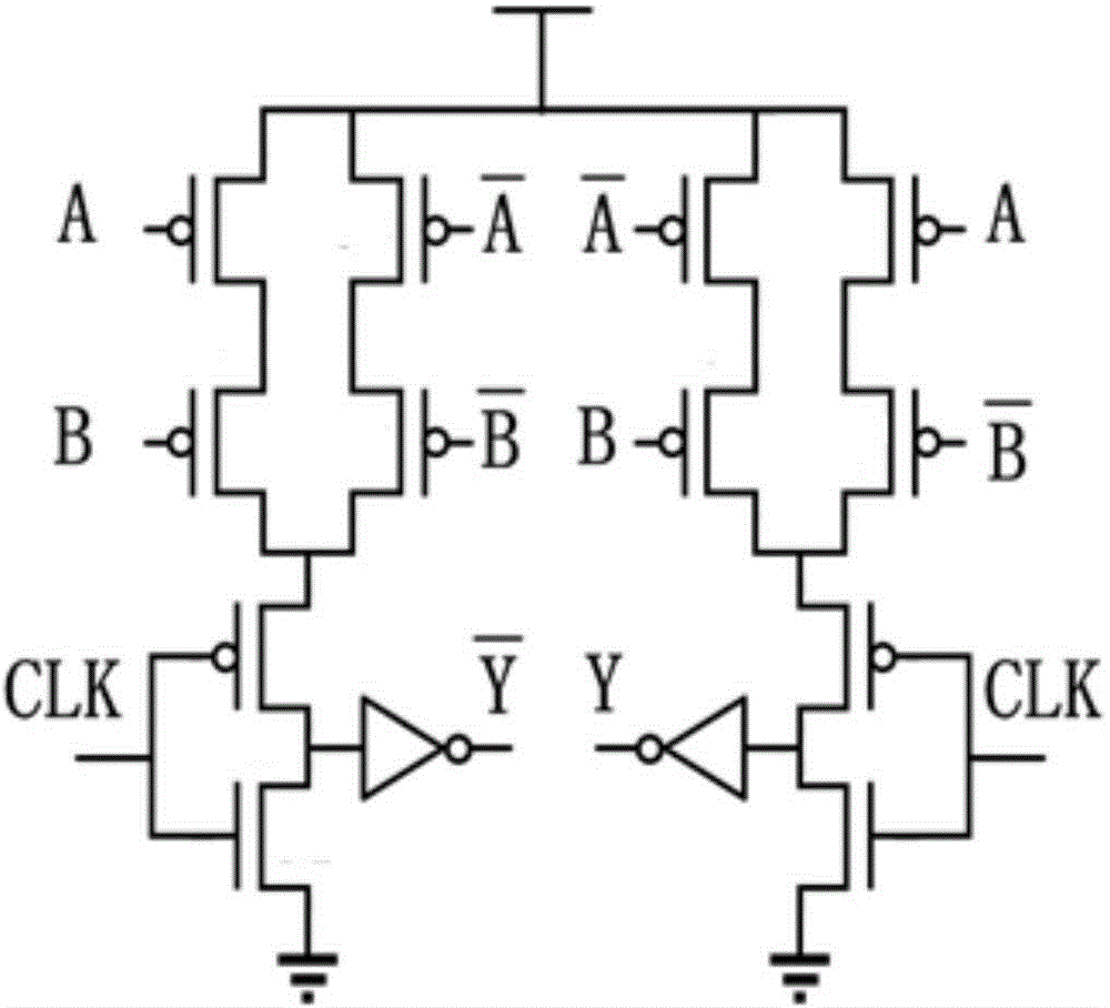
[0051] The present invention provides a delay-based dual-rail precharge logic NAND gate circuit, which is characterized in that it includes PMOS transistors P1, P2, P3, P4, P5, P6, NMOS transistors N1, N2, N3, the first inverting device F1; the second inverter F2, such as figure 2 shown.

[0052] The source of the PMOS transistor P1 is connected to the power supply, the gate is connected to the clock signal, and the drain is connected to the source of the PMOS transistor P2; the drain of the PMOS transistor P2 is connected to the source of the PMOS transistor P3, so The drain of the PMOS transistor P3 is connected to the drain of the NMOS transistor N1 and the input terminal of the first inverter F1; the g...


PUM


Abstract

The invention discloses a time delay-based double-track pre-charge logic NAND gate circuit and a time delay-based double-track pre-charge logic exclusive or gate circuit. By transforming positions of PMOS (P-channel metal oxide semiconductor) transistors or NMOS (N-channel metal oxide semiconductor) transistors in the time delay-based double-track pre-charge logic NAND gate circuit and the time delay-based double-track pre-charge logic exclusive or gate circuit in the prior art and increasing or decreasing the PMOS transistors or the NMOS transistors, the improvement of the NAND gate circuit and the exclusive or gate circuit is realized; the improved NAND gate circuit and the improved exclusive or gate circuit area capable of realizing more balanced power consumption, faster speed and lower power consumption, and can better resist differential power attack.

Description

technical field [0001] The present invention relates to the technical field of integrated circuits, and more specifically to a delay-based dual-rail precharge logic NAND circuit and an exclusive OR gate circuit. Background technique [0002] With the development of informatization and information industry, VLSI and computer technology are widely used in various fields of society. A large number of confidential systems have been established on the basis of the information industry, and the security of information systems has become a key issue that governments and various large organizations must pay attention to. Information security refers to the protection of software and hardware systems based on information systems and the data stored in the systems from being stolen, changed or even destroyed by the outside world. [0003] All information technology operations, including information encryption, are realized on the corresponding physical basis, but these physical founda...

Claims


Application Information

Patent Timeline
IPC IPC(8): H03K19/20
Inventor 贾嵩王子一刘黎王源张钢刚
Owner PEKING UNIV
Why Eureka
Try Eureka