Transistor forming method

A transistor, wet etching technology, applied in semiconductor/solid-state device manufacturing, electrical components, circuits, etc., can solve problems affecting transistor performance, and achieve the effect of improving performance, flattening the surface, and reducing the etching rate

A transistor, wet etching technology, applied in semiconductor/solid-state device manufacturing, electrical components, circuits, etc., can solve problems affecting transistor performance, and achieve the effect of improving performance, flattening the surface, and reducing the etching rate

CN104701167AActive Publication Date: 2015-06-10SEMICON MFG INT (SHANGHAI) CORP

Image

  • Transistor forming method
  • Transistor forming method
  • Transistor forming method

Examples


Embodiment Construction

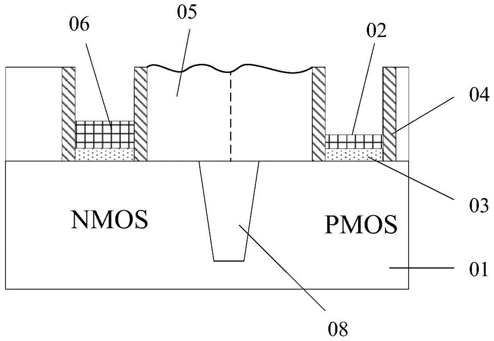
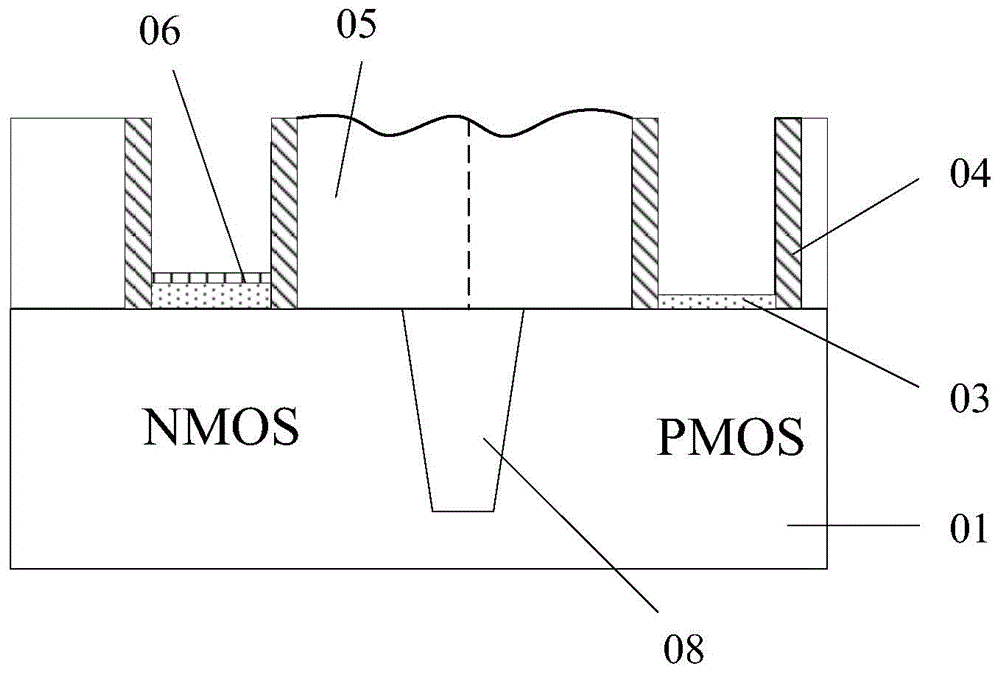
[0037] In the step of removing dummy gates in the metal gate formation process of transistors in the prior art, the dummy gates have different heights in areas where dummy gates are densely packed and where dummy gates are loose. The top surface of the gate is also uneven, so that after the dry etching of the dummy gate, the thickness of the remaining dummy gate is not uniform, and the residual dummy gate in the thicker part is The etching may not be clean, or the substrate under the dummy gate in the thinner part is damaged by wet etching.

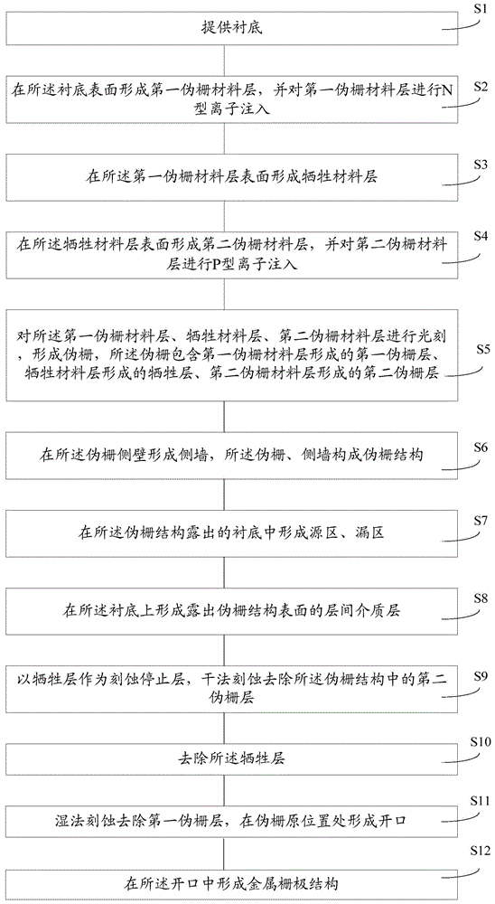
[0038] In order to solve the above technical problems, the present invention provides a method for forming a transistor. In the process of forming a dummy gate, a three-layer transistor consisting of a first dummy gate layer, a sacrificial layer and a second dummy gate layer is formed from bottom to top. The dummy gate, wherein the sacrificial layer is used as an etch stop layer of the second dummy gate layer, can make the surface thickne...


PUM


Abstract

The invention provides a transistor forming method. The method includes forming a first false grid layer, a sacrificial layer and a second false grid layer on a substrate from bottom to top; forming a side wall on the side wall of a false grid, and obtaining a false grid structure comprising the false grid and the side wall; forming a source region and a leak region in the substrate; forming an interlayer medium layer exposing the surface of the false grid structure; allowing the sacrificial layer to serve as an etching stop layer, and removing the second false grid layer of the false grid structure by dry etching; removing the sacrificial layer; removing the first false grid layer by wet etching, and forming an opening; forming a metal grid electrode structure in the opening. The method has the advantages that the influence of the substrate during false grid removal is small, and the quality of a formed transistor is improved.

Description

technical field [0001] The present invention relates to the field of semiconductors, in particular to a method for forming a transistor. Background technique [0002] In the high-K dielectric / metal gate-last engineering of transistors, the gate-last process is generally used to form the metal gate. According to the existing gate-last process, a dummy gate structure is first formed, and then the dummy gate is removed, and a metal gate is formed in the opening created by removing the dummy gate. The feature sizes of various semiconductors manufactured by the current process are very small, and it is quite difficult to completely remove the dummy gate in such a small dummy gate structure. In the prior art, dry etching and wet etching are generally used to remove the dummy gate. [0003] However, the dry etching and wet etching used to remove the dummy gates have the following problems. Because in the wafer, the height of the dummy gates is different in the area where the dummy...

Claims


Application Information

Patent Timeline
10 Jun 2015
Publication
CN104701167A
IPC
H01L21/336
Inventors
曾以志; 隋运奇