Manufacturing method for increasing effective photosensitive area of photoelectric material

A photosensitive area and photoelectric material technology, which is applied in the field of preparation of multi-period micro-nano composite structures, can solve the problems of not being suitable for mass production, strict use conditions, poor uniformity, etc., and achieve improved photoelectric conversion efficiency, increased contact area, and easy operation Effect

Active Publication Date: 2015-06-17
CHANGCHUN UNIV OF SCI & TECH
View PDF10 Cites 4 Cited by
  • Summary
  • Abstract
  • Description
  • Claims
  • Application Information

AI Technical Summary

Problems solved by technology

These technologies and methods either use time-consuming sequential work methods, and the processing speed for multi-cycle mixed structures is very slow, which is not suitable for mass production; o

Method used


Image

  • Manufacturing method for increasing effective photosensitive area of photoelectric material
  • Manufacturing method for increasing effective photosensitive area of photoelectric material
  • Manufacturing method for increasing effective photosensitive area of photoelectric material

Examples


Embodiment 1

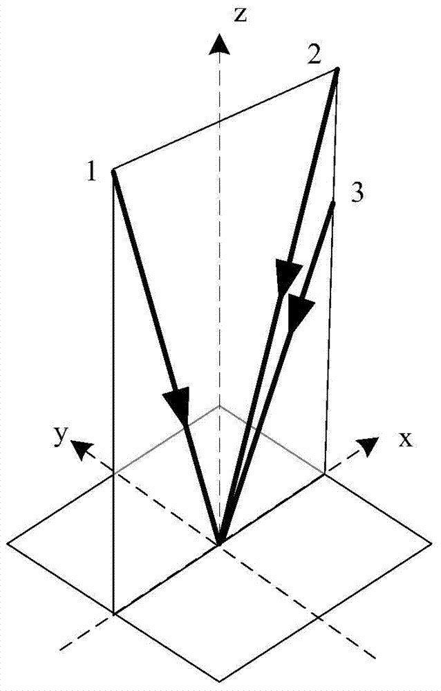
[0024] Using the optical path of the three-beam laser interference system, the laser wavelength is 1.064μm, the energy density of each beam is 0.64J / cm2, and the pulse width is 6ns. The incident mode of the three laser beams is as follows figure 1 As shown, the incident angles of beam 1 and beam 2 are both 7°, the incident angle of beam 3 is 14°, the spatial angle of beam 1 is 0°, the spatial angle of beam 2 and beam 3 is 180°, the three beams The polarization state is the same, and the polished single crystal silicon surface is exposed for 10s. After the first exposure is completed, the rotating table is rotated 90° clockwise for the second exposure. The exposure time is 8s, and the following is obtained: image 3 The square composite structure has a side length of 4.4 μm, a structure depth of 0.2-1 μm, a modulation period of 8.7 μm, and a 15% increase in the surface area of ​​the material.

Embodiment 2

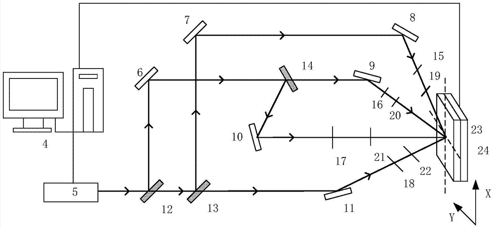
[0026] The optical path of the four-beam laser interference system is as follows: figure 2 As shown, the laser wavelength is 1.064μm, the energy density of each beam is 0.64J / cm2, the pulse width is 6ns, the incident angle of the four beams is 8°, and the space angles of the four beams are 0°, 90°, 180 °, 270°, the exposure time on the surface of polished single crystal silicon material is 5s, and the obtained Figure 4 The lattice structure shown is similar to a raised hemisphere with a period of 4 μm, the size of a single protrusion is 2-2.5 μm, the depth of the structure is 0.1-0.32 μm, and the surface area of ​​the material is increased by 30%.

[0027] In a word, the present invention utilizes modulating laser interference lithography technology to directly prepare a multi-period micro-nano composite structure on the surface of a matrix material or a photosensitive material, and adds a three-dimensional optical contact surface within a two-dimensional unit plane area. Ac...


PUM

PropertyMeasurementUnit
Sizeaaaaaaaaaa
Energy densityaaaaaaaaaa
Pulse widthaaaaaaaaaa

Abstract

The invention discloses a manufacturing method for increasing the effective photosensitive area of a photoelectric material. The manufacturing method comprises the steps that three laser beams with modulation performance are utilized for carrying out interfering and photoetching on the surface of a host material or the photosensitive material, multi-periodicity micro-nano composite structures in different shapes and of different structures are obtained and manufactured through the mode of multi-angle overlapping exposure or movable distance overlapping exposure, multiple laser beams with the modulation performance can be utilized for carrying out interfering and photoetching on the surfaces of the materials, the multi-periodicity micro-nano composite structures can be directly manufactured, and the three-dimensional effective photosensitive area is increased in a two-dimensional unit plane .

Description

technical field [0001] The invention relates to a preparation method for increasing the effective photosensitive area of ​​a photoelectric material, in particular to a preparation of a multi-period micro-nano composite structure that increases the effective photosensitive area with high efficiency and low cost, and can be applied to solar cells, LEDs, etc. In semiconductor devices, it also provides an advanced preparation technology for the manufacture of new devices and new materials. Background technique [0002] Since the end of the last century, the progress of new high-performance materials, devices and systems has always relied on the development of micro-nano manufacturing technology. With the continuous deepening of research on nano-manufacturing technology, the fabrication of micro-nano multi-scale composite structures has become a key problem to be solved urgently. In recent years, the superhydrophobic self-cleaning properties and wide-spectrum wide-angle anti-ref...

Claims


Application Information

Patent Timeline
IPC IPC(8): B23K26/00B23K26/064G03F7/20
CPCG03F7/2053H01L31/02363Y02P70/50
Inventor 王作斌董莉彤曹亮于淼胡尧威徐佳宋正勋翁占坤
Owner CHANGCHUN UNIV OF SCI & TECH
Why Eureka
Try Eureka