Semiconductor structure and forming method thereof

A semiconductor and transistor technology, applied in the field of semiconductor structure and its formation, can solve the problems affecting the performance of fin field effect transistors, source and drain punch-through of source and drain regions, etc., and achieve good surface morphology, stable performance and improved performance. Effect

Active Publication Date: 2015-06-24
SEMICON MFG INT (SHANGHAI) CORP
View PDF5 Cites 10 Cited by
  • Summary
  • Abstract
  • Description
  • Claims
  • Application Information

AI Technical Summary

Problems solved by technology

[0006] However, in the existing FinFET, source-drain punch-through is prone to occur between the source region and the drain region, which affects the performance of the FinFET.

Method used


Image

  • Semiconductor structure and forming method thereof
  • Semiconductor structure and forming method thereof
  • Semiconductor structure and forming method thereof

Examples


Embodiment Construction

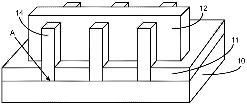
[0034] As mentioned in the background, in the existing FinFET, source-drain punch-through is prone to occur between the source region and the drain region, which affects the performance of the FinFET.

[0035] After research, please continue to refer to figure 1 In order to enable the fins 14 covered by the gate structure 12 to form channel regions, the distance from the bottom of the source region and the drain region in the fins 14 to the top of the fins 14 is relatively large, so that the fins formed in the fins The channel region on the sidewall of 14 can also be driven by the source region and the drain region. However, when the distance from the bottom of the source region and the drain region to the top of the fin 14 is relatively large, the control ability of the gate structure 12 on the top of the fin 14 to the bottom of the source region and the drain region is relatively low, so that the source and drain regions Punch-through occurs at the bottom of the drain regio...


PUM


Abstract

The invention discloses a semiconductor structure and a forming method thereof. The semiconductor structure forming method comprises steps: a substrate is provided, wherein the substrate is provided with a first region, and the surface of the substrate in the first region is provided with a first fin part; dielectric layers are formed on the surface of the substrate and the surface of the side wall of the first fin part, wherein the surface of the dielectric layer is lower than the top part of the first fin part; a first anti-damage injection process is carried out on the bottom part of part of the first fin part exposed out of the dielectric layer, ion implantation damages to the first fin part can be prevented due to the first anti-damage injection process, a first anti-penetrating layer is formed in the first fin part, and the position of the first anti-penetrating layer is corresponding to the surface of the dielectric layer. Performance of the formed semiconductor structure is improved.

Description

technical field [0001] The invention relates to the technical field of semiconductor manufacturing, in particular to a semiconductor structure and a forming method thereof. Background technique [0002] With the rapid development of semiconductor manufacturing technology, semiconductor devices are developing towards higher element density and higher integration. As the most basic semiconductor device, transistors are currently being widely used. Therefore, with the increase of component density and integration of semiconductor devices, the gate size of planar transistors is getting shorter and shorter. The ability of traditional planar transistors to control channel current Weakened, resulting in short channel effect, resulting in leakage current, and ultimately affecting the electrical performance of semiconductor devices. [0003] In order to overcome the short-channel effect of the transistor and suppress the leakage current, a Fin Field Effect Transistor (Fin FET) is pr...

Claims


Application Information

Patent Timeline
Patent Type & Authority Applications(China)
IPC IPC(8): H01L21/336H01L29/78H01L29/10
CPCH01L29/66795H01L29/7854
Inventor 谢欣云
Owner SEMICON MFG INT (SHANGHAI) CORP
Why Eureka
Try Eureka