

A sputtering system
A sputtering system and sputtering source technology, applied in the field of sputtering systems, can solve the problems of reducing deposition rate, affecting production efficiency, etc., and achieve the effects of increasing sputtering rate, quality, and film-forming rate
- Summary
- Abstract
- Description
- Claims
- Application Information
AI Technical Summary
Problems solved by technology
Method used
Image

Examples
Embodiment Construction
[0023] In order for those skilled in the art to better understand the technical solution of the present invention, the sputtering system provided by the present invention will be described in detail below with reference to the accompanying drawings.
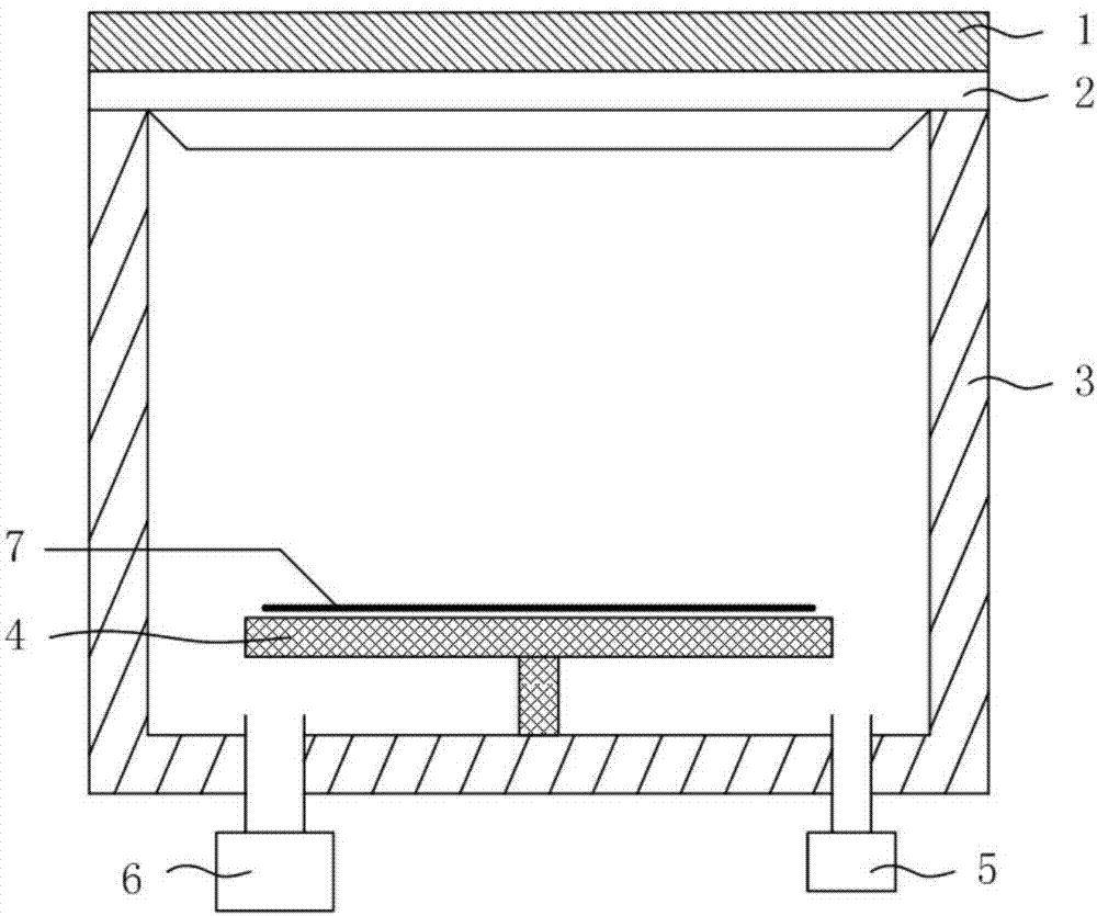
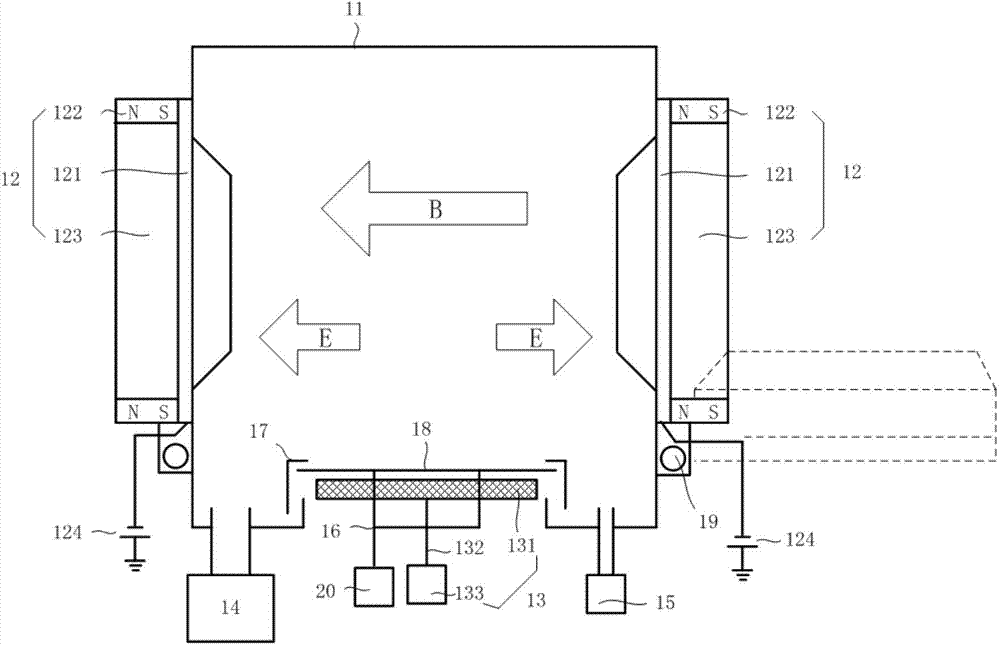
[0024] figure 2 It is a schematic structural diagram of a sputtering system according to an embodiment of the present invention. Such as figure 2 As shown, the sputtering system includes a chamber 11 , a sputtering source 12 , a susceptor 13 , a vacuum system 14 and a process gas supply system 15 . The sputtering source 12 is arranged on the sidewall of the chamber 11, the base 13 is arranged on the bottom in the chamber 11, the vacuum system 14 is used to adjust the vacuum degree in the chamber 11, and the process gas supply system 15 is used to supply the chamber 11 Provide the process gas needed to implement the process, such as Ar gas.
[0025] The sputtering system of this embodiment is provided with two sputtering sour...
PUM
 Abstract
Description
Claims
Application Information