Method for improving appearance quality of rear surface of thin sheet

A technology of apparent quality and flakes, which is applied in the direction of electrical components, semiconductor/solid-state device manufacturing, circuits, etc., and can solve problems such as poor apparent quality and easy metal peeling

Inactive Publication Date: 2015-07-01
SUZHOU TONGGUAN MICROELECTRONICS
View PDF3 Cites 8 Cited by
  • Summary
  • Abstract
  • Description
  • Claims
  • Application Information

AI Technical Summary

Problems solved by technology

[0006] The purpose of the present invention is that the present invention provides a cleaning method for improving the apparent quality of the backside of the thinned sheet, which is used to improve the frequent occurrence of subsequent processes of the wafer after thinning by a low-mesh grinding wheel (usually 300 mesh, 600 mesh). Poor apparent quality such as imprints and smudges and easy peeling off of the metal on the back

Method used


Image

  • Method for improving appearance quality of rear surface of thin sheet
  • Method for improving appearance quality of rear surface of thin sheet
  • Method for improving appearance quality of rear surface of thin sheet

Examples


Embodiment 1)

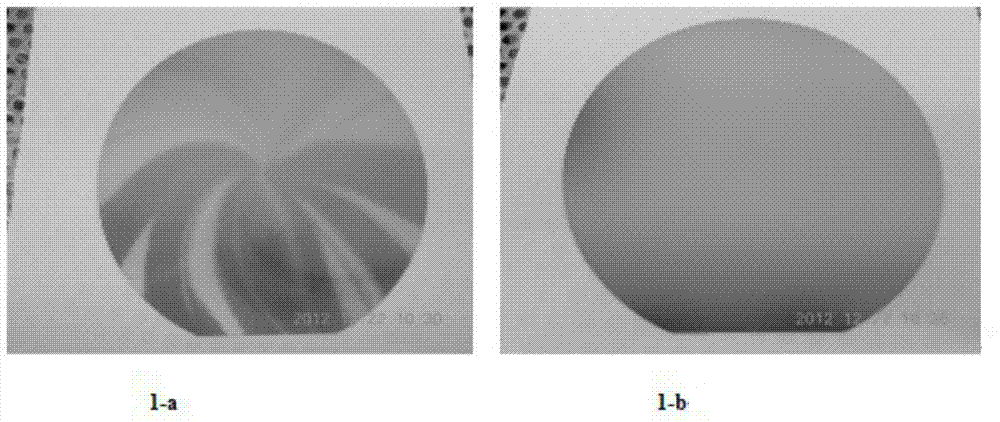
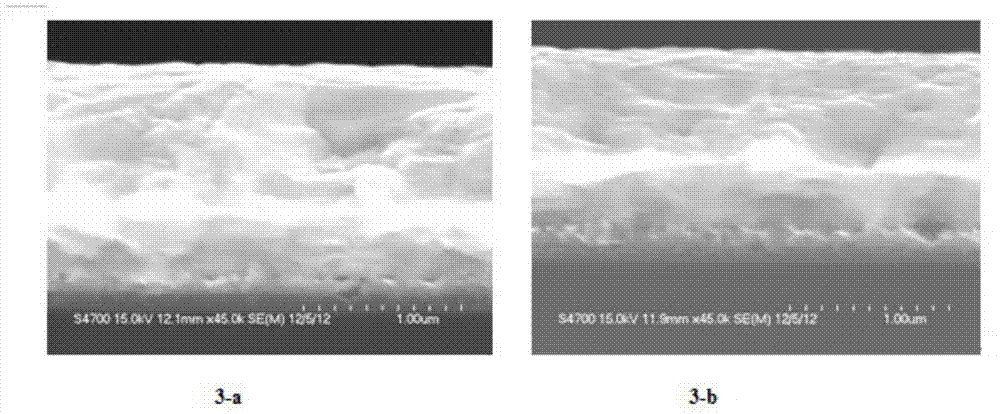
[0028] See figure 1 , 2 、3

[0029] Follow the steps below:

[0030] 1. Apply a film to the front of the wafer to protect the front of the wafer, and the film used is required to have certain acid corrosion resistance;

[0031] 2. Use a 300-mesh grinding wheel and a 600-mesh grinding wheel to thin the wafer processed in step 1 to obtain a thin slice of the required thickness (usually 160um ~ 350um);

[0032] 3. Put the wafer processed in step 2 into the mixed solution according to the volume ratio of hydrofluoric acid (HF): nitric acid (HNO3): glacial acetic acid (CH3COOH) = 1:7:7, and the solution temperature is 25 When ℃~28℃, corrode for 30 seconds;

[0033] 4. Rinse the slices processed in step 3 in deionized water, and after the flushing is completed, perform drying treatment in a dryer with deionized water and nitrogen environment;

[0034] 5. Perform ion implantation on the back side of the slice processed in step 4;

[0035] 6. Carrying out film removal treatment ...

Embodiment 2)

[0042] Follow the steps below:

[0043] 1. Apply a film to the front of the wafer to protect the front of the wafer, and the film used is required to have certain acid corrosion resistance;

[0044] 2. Use a 300-mesh grinding wheel and a 600-mesh grinding wheel to thin the wafer processed in step 1 to obtain a thin slice of the required thickness (usually 160um ~ 350um);

[0045] 3. Put the wafer processed in step 2 into the mixed solution according to the volume ratio of hydrofluoric acid (HF): nitric acid (HNO3): glacial acetic acid (CH3COOH) = 1:7:7, and the solution temperature is 26 When ℃~30℃, corrode for 80 seconds;

[0046] 4. Rinse the slices processed in step 3 in deionized water, and after the flushing is completed, perform drying treatment in a dryer with deionized water and nitrogen environment;

[0047] 5. Perform ion implantation on the back side of the slice processed in step 4;

[0048] 6. Carrying out film removal treatment to the sheet processed in step 5...
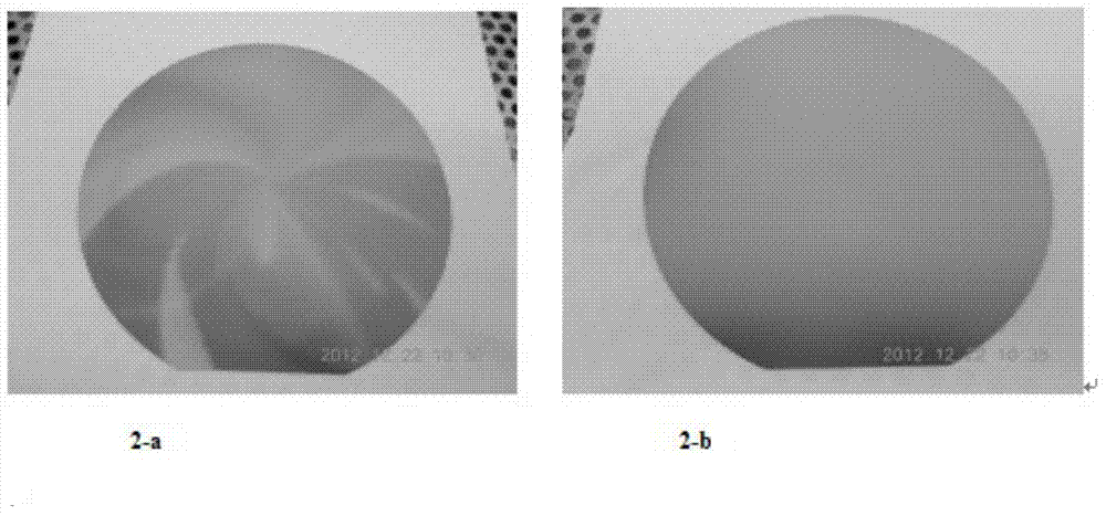
Embodiment 3)

[0055] Follow the steps below:

[0056]1. Apply a film to the front of the wafer to protect the front of the wafer, and the film used is required to have certain acid corrosion resistance;

[0057] 2. Use a 300-mesh grinding wheel and a 600-mesh grinding wheel to thin the wafer processed in step 1 to obtain a thin slice of the required thickness (usually 160um ~ 350um);

[0058] 3. Put the wafer processed in step 2 into the mixed solution according to the volume ratio of hydrofluoric acid (HF): nitric acid (HNO3): glacial acetic acid (CH3COOH) = 1:7:7, and the solution temperature is 28 When ℃~30℃, corrode for 1300 seconds;

[0059] 4. Rinse the slices processed in step 3 in deionized water, and after the flushing is completed, perform drying treatment in a dryer with deionized water and nitrogen environment;

[0060] 5. Perform ion implantation on the back side of the slice processed in step 4;

[0061] 6. Carrying out film removal treatment to the sheet processed in step ...


PUM


Abstract

The invention relates to a method for improving appearance quality of a rear surface of a thin sheet. The method comprises the steps of adhering a film on the front surface; thinning the rear surface; corroding the rear surface through silicon; removing the film; washing the rear surface; metalizing the rear surface; the thinned sheet is corroded through corrosion liquid during performing the rear surface silicon corrosion process and the process of removing silicon dioxide before metalizing the rear surface, wherein the corrosion liquid in the rear surface silicon corrosion process is prepared from the following components in volume ratio: hydrofluoric acid, nitric acid and glacial acetic acid in volume ratio of 1: 7: 1; the corrosion liquid in the process of removing silicon dioxide before metalizing the rear surface is prepared from the following components in volume ratio: BOE and C2H6O2 in volume ratio of 1: 1.5. A wafer processed by the method has the advantages that the rear surface metal surface is free of curling, tilting and other phenomena after finishing the following rear surface metalizing process; the phenomenon of failure of the reliability of a semiconductor caused by the spalling of the rear surface metal layer can be avoided; meanwhile, the appearance condition is obviously superior to that of other wafers processed by other washing manner.

Description

technical field [0001] The invention relates to the technical field of semiconductor manufacturing technology, in particular to a method for cleaning the back of a thinned sheet used in the semiconductor manufacturing process. Background technique [0002] The semiconductor industry is currently one of the fastest growing and most influential industries in the world. With the rapid development of the semiconductor industry, semiconductor chips have been widely used in the semiconductor field, especially in switching power supplies, frequency converters, household appliances, It is more widely used in electronic equipment such as smart cards, personal digital assistants, and aerospace. Ultra-thin power devices represented by VDMOS and IGBT are playing an increasingly important role. [0003] In the manufacturing process of ultra-thin chips, the post-processing process of wafers is usually as follows: [0004] Front film - back thinning - back silicon etching - back ion impl...

Claims


Application Information

Patent Timeline
Patent Type & Authority Applications(China)
IPC IPC(8): H01L21/02H01L21/306
CPCH01L21/02082H01L21/02041H01L21/30604
Inventor 张海欧
Owner SUZHOU TONGGUAN MICROELECTRONICS
Why Eureka
Try Eureka