Semiconductor device and forming method thereof

A semiconductor and device technology, applied in the field of semiconductor devices and their formation, can solve the problems of reducing the reliability of semiconductor devices, reducing the turn-on current of semiconductor devices, and the surge of leakage current, so as to avoid the problem of source-drain punch-through and reduce hot carriers effect, the effect of optimizing electrical performance

Active Publication Date: 2015-07-01
SEMICON MFG INT (SHANGHAI) CORP
View PDF6 Cites 6 Cited by
  • Summary
  • Abstract
  • Description
  • Claims
  • Application Information

AI Technical Summary

Problems solved by technology

When the source-drain is punched through, the leakage current surges, causing the gate electrode to lose control of the channel
In addition, the high electric field at the boundary of the drain terminal can also cause hot carrier effects, reduce the reliability of semiconductor devices, and reduce the turn-on current of semiconductor devices

Method used


Image

  • Semiconductor device and forming method thereof
  • Semiconductor device and forming method thereof
  • Semiconductor device and forming method thereof

Examples


Embodiment Construction

[0035] It can be seen from the background art that increasing the turn-on current of the semiconductor device and reducing the leakage current are urgent problems to be solved.

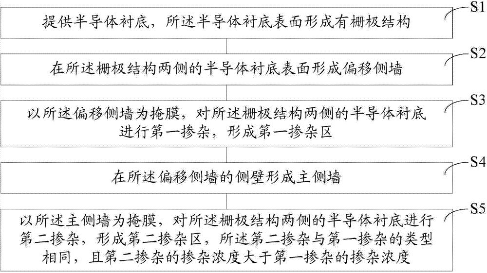
[0036] In order to solve the above problems, the formation method of the semiconductor device is studied. The formation method of the semiconductor device includes the following steps, please refer to figure 1 : Step S1, providing a semiconductor substrate, the surface of the semiconductor substrate is formed with a gate structure; Step S2, forming offset spacers on the surface of the semiconductor substrate on both sides of the gate structure; Step S3, using the offset Shifting the sidewalls as a mask, performing first doping on the semiconductor substrates on both sides of the gate structure to form a first doped region; step S4, forming main sidewalls on the sidewalls of the offset sidewalls; Step S5, using the main sidewall as a mask, performing second doping on the semiconductor substrates on bot...


PUM


Abstract

A semiconductor device and a forming method thereof are provided. The forming method of the semiconductor device comprises the following steps: providing a semiconductor substrate; performing first doping on the semiconductor substrate to form a first doped region; forming a patterned mask layer on the surface of the semiconductor substrate, wherein the patterned mask layer has an opening which exposes the surface of the semiconductor substrate; etching part of the semiconductor substrate in the thickness direction with the patterned mask layer as a mask to form a groove in the semiconductor substrate; and performing second doping on the semiconductor substrate to form a second doped region, wherein the first doping and the second doping are of the same doping type, the doping concentration of the second doping is greater than the doping concentration of the first doping, and the second doped region and the first doped region are connected. By adopting the method of the invention, the opening current of the semiconductor device is increased, the leakage current is reduced, and the electrical performance of the semiconductor device is improved.

Description

technical field [0001] The invention relates to the technology in the field of semiconductor manufacturing, in particular to a semiconductor device and a forming method thereof. Background technique [0002] With the rapid development of Ultra Large Scale Integration (ULSI: Ultra Large Scale Integration), the manufacturing process of integrated circuits has become more and more complex and sophisticated. In order to improve integration and reduce manufacturing costs, the critical dimensions of semiconductor devices continue to decrease, and the number of semiconductor devices per unit area of ​​a chip continues to increase. While the critical dimensions of semiconductor devices are reduced, the patterns of semiconductor devices are also continuously miniaturized. [0003] With the continuous reduction of critical dimensions of semiconductor devices, the distance between the source and drain of semiconductor devices is getting shorter and shorter. As the drain voltage continu...

Claims


Application Information

Patent Timeline
Patent Type & Authority Applications(China)
IPC IPC(8): H01L21/336H01L21/28H01L29/10H01L29/78H01L29/08H01L29/423H01L29/06
CPCH01L29/1083H01L29/4236H01L29/66477H01L29/78
Inventor 刘金华
Owner SEMICON MFG INT (SHANGHAI) CORP
Why Eureka
Try Eureka