Semiconductor device and forming method thereof

A semiconductor and device technology, applied in the field of semiconductor devices and their formation, can solve problems such as peeling off of multi-layer pseudo-plug layers and multi-layer pseudo-metal layers, reduction of insulation isolation performance of interlayer dielectric layers, instability of oscillation circuits, etc., to achieve The texture is dense, the insulation performance is good, and the effect of ensuring the insulation performance is ensured

Active Publication Date: 2015-07-01
SEMICON MFG INT (SHANGHAI) CORP
View PDF5 Cites 6 Cited by
  • Summary
  • Abstract
  • Description
  • Claims
  • Application Information

AI Technical Summary

Problems solved by technology

[0003] However, in the prior art, the multi-layer dummy plug layer and the multi-layer dummy metal layer on the edge of the wafer are peeled off
The peeled dummy plug layer and dummy metal layer are scattered on the surface of the interlayer dielectric layer where they are located, which will cause signal crosstalk to the plug layer and interconnection metal layer of the same layer, and reduce the insulation isolation performance of the interlayer dielectric layer
For example, in an oscillating circuit, the peeled dummy plug layer and dummy metal layer will induce electromagnetic signals, which will cause the oscillating circuit to be unstable

Method used


Image

  • Semiconductor device and forming method thereof
  • Semiconductor device and forming method thereof
  • Semiconductor device and forming method thereof

Examples


Embodiment Construction

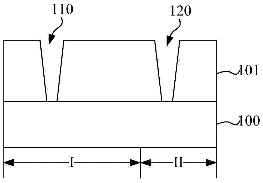
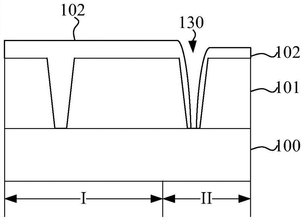
[0047] Aiming at the problems existing in the prior art, the inventor conducted an analysis and found that: after the device structure is formed in the wafer, the first contact hole corresponding to the device region and the first contact hole on the edge of the wafer are formed in the first dielectric layer on the wafer. The second contact hole, followed by chemical vapor deposition of tungsten metal, tungsten will fill in the first contact hole and the second contact hole, and cover the first dielectric layer.

[0048] On the one hand, during the process of depositing tungsten, the wafer will be placed on the base, and the edge of the wafer will be covered by the shielding part on the base but the shielding part will not be in contact with the wafer. Tungsten diffuses in the reaction chamber in gaseous phase, but the second contact hole is covered, and tungsten enters the second contact hole through the gap between the shielding part and the second contact hole, so that the t...


PUM


Abstract

A semiconductor device and a forming method thereof are provided. The forming method of the semiconductor device comprises the following steps: providing a wafer which is divided into a device region and a wafer edge; forming a first dielectric layer on the wafer; forming a first contact hole corresponding to the device region and a second contact hole corresponding to the wafer edge in the first dielectric layer; forming a conductive layer which covers the first dielectric layer, fills the first contact hole completely and fills the second contact hole, wherein the conductive layer in the second contact hole is provided with a hole communicating the opening with the bottom of the second contact hole; forming a filling layer which covers the conductive layer and fills the hole completely; and removing the conductive layer and the filling layer on the first dielectric layer, wherein the remaining conductive layer in the first contact hole is used as a first plug layer, and the remaining filling layer and the reaming conductive layer in the second contact hole are used as a first pseudo plug layer. The first pseudo plug layer can bear large stress, and multiple dummy plug layers and pseudo metal layers do not peel off. Thus, the first dielectric layer has better insulation isolation performance.

Description

technical field [0001] The invention relates to the technical field of semiconductors, in particular to a semiconductor device and a forming method thereof. Background technique [0002] In the field of semiconductor technology, usually after a device structure is formed in a wafer, a multi-layer interconnection metal layer and a plug layer between two adjacent interconnection metal layers are formed on the wafer. Wherein, the plug layer corresponding to the device area of ​​the wafer electrically connects the device structure and the interconnection metal layer, and electrically connects the two interconnection metal layers. However, when forming the plug layer and the interconnection metal layer in the device area, a dummy plug layer and a dummy metal layer are also formed on the non-device area at the edge of the wafer, wherein the edge of the wafer is in the range of 1-3 μm from the wafer boundary wafer area. In the prior art, since the mask that defines the position o...

Claims


Application Information

Patent Timeline
Patent Type & Authority Applications(China)
IPC IPC(8): H01L21/768H01L21/762
CPCH01L21/76838H01L21/76843H01L23/5226H01L2221/1073
Inventor 张继伟李志超蒋剑勇林保璋
Owner SEMICON MFG INT (SHANGHAI) CORP
Why Eureka
Try Eureka