
Common-gate stereoscopic CMOS (Complementary Metal-Oxide-Semiconductor Transistor) device, OLED (Organic Light Emitting Diode) device and manufacturing method thereof

A manufacturing method and three-dimensional technology, which are applied in semiconductor/solid-state device manufacturing, semiconductor devices, electric solid-state devices, etc., can solve the problems of complex manufacturing process flow, complex device structure and high cost

Inactive Publication Date: 2015-07-01
KUNSHAN GO VISIONOX OPTO ELECTRONICS CO LTD
View PDF3 Cites 14 Cited by
  • Summary
  • Abstract
  • Description
  • Claims
  • Application Information

AI Technical Summary

Problems solved by technology

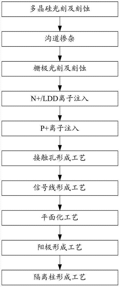
The above-mentioned CMOS manufacturing process requires a total of 4 ion implantation processes, at least 11 photolithography processes, and correspondingly requires at least 11 photomasks. The device structure is complex, the occupied area is large, and the manufacturing process is complicated and the cost is relatively high.

Method used


Image

  • Common-gate stereoscopic CMOS (Complementary Metal-Oxide-Semiconductor Transistor) device, OLED (Organic Light Emitting Diode) device and manufacturing method thereof
  • Common-gate stereoscopic CMOS (Complementary Metal-Oxide-Semiconductor Transistor) device, OLED (Organic Light Emitting Diode) device and manufacturing method thereof
  • Common-gate stereoscopic CMOS (Complementary Metal-Oxide-Semiconductor Transistor) device, OLED (Organic Light Emitting Diode) device and manufacturing method thereof

Examples


Embodiment Construction

[0017] The following introduces some of the possible embodiments of the present invention, which are intended to provide a basic understanding of the present invention, but are not intended to identify key or decisive elements of the present invention or limit the scope of protection. It is easy to understand that, according to the technical solution of the present invention, those skilled in the art may propose other alternative implementation manners without changing the essence and spirit of the present invention. Therefore, the following specific embodiments and drawings are only exemplary descriptions of the technical solution of the present invention, and should not be regarded as the entirety of the present invention or as a limitation or restriction on the technical solution of the present invention.

[0018] In the drawings, the thicknesses of layers and regions are exaggerated for clarity, and shape features such as roundness due to etching are not illustrated in the ...


PUM


Abstract

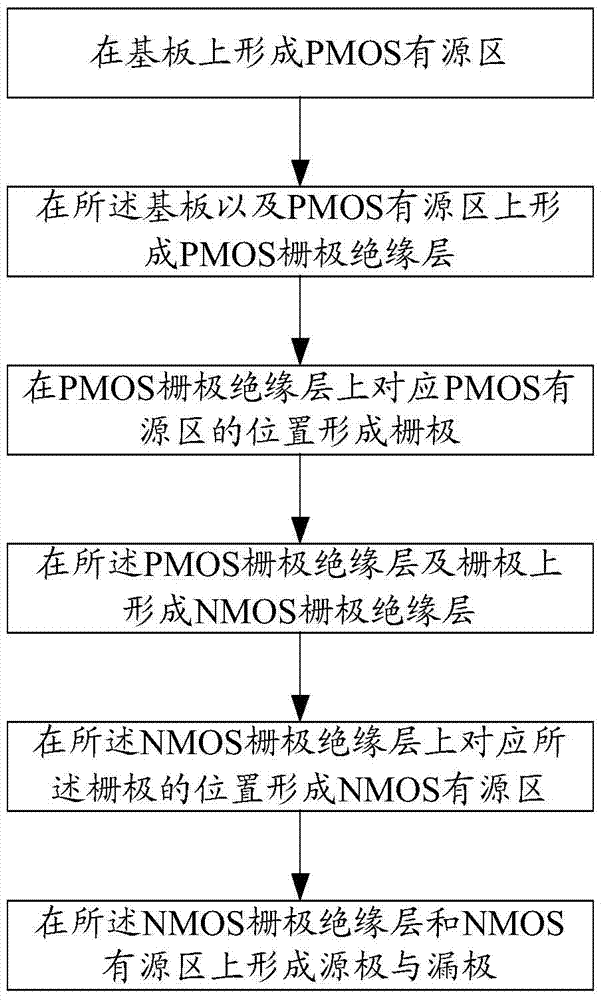
The invention provides a common-gate stereoscopic CMOS (Complementary Metal-Oxide-Semiconductor Transistor) device, an OLED (Organic Light Emitting Diode) device and a manufacturing method thereof. In the common-gate stereoscopic CMOS device, an NMOS transistor adopts an oxide semiconductor device, a PMOS transistor adopts an LTPS device, the PMOS transistor and the NMOS transistor share a gate, sources and drains of the two are formed through one etching process, the PMOS transistor and the NMOS transistor are arranged in a stacking mode, the occupied area can be effectively reduced, the integration degree of a circuit is improved, and the CMOS device and the LED device manufacturing process is simple and the cost is low.

Description

technical field [0001] The invention relates to the field of organic electroluminescent devices, in particular to a common gate three-dimensional CMOS device, an OLED device and a manufacturing method thereof. Background technique [0002] In flat panel display technology, organic light-emitting diodes (Organic Light-Emitting Diode, referred to as OLED) have many advantages such as thinness, active light emission, fast response speed, wide viewing angle, rich colors and high brightness, low power consumption, high and low temperature resistance, etc. It is recognized by the industry as the third-generation display technology following the liquid crystal display (LCD). [0003] According to the way of light emission, OLED is divided into bottom-emitting device (Bottom Organic Light-emitting Device, referred to as BEOLED) and top-emitting device (TOP Organic Light-emitting Device, referred to as TEOLED). According to the driving method, OLED is divided into passive organic li...

Claims


Application Information

Patent Timeline
IPC IPC(8): H01L27/092H01L27/32H01L21/77
CPCH01L27/1225
Inventor 卜维亮
Owner KUNSHAN GO VISIONOX OPTO ELECTRONICS CO LTD
Learn More