Failure testing circuit and method of power device
A technology for failure testing and power devices, which is applied in the field of power electronics and can solve problems such as chip burnout
- Summary
- Abstract
- Description
- Claims
- Application Information
AI Technical Summary
Problems solved by technology
Method used
Image

Examples
Embodiment 1
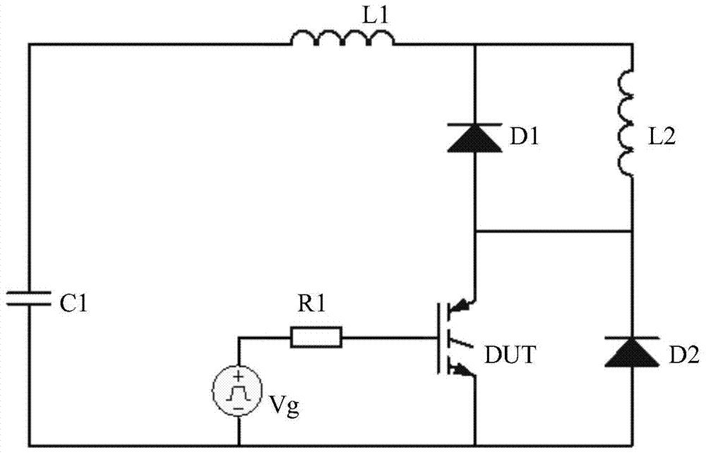
[0035] figure 1 A schematic diagram of an existing IGBT short-circuit safe working area test circuit is shown.
[0036] Such as figure 1 As shown, the existing IGBT short-circuit safe operating area test circuit includes a capacitor C1, a parasitic inductance L1, diodes D1 and D2, a load inductance L2, a controller Vg, and a resistor R1 connected in series between the controller Vg and the IGBT gate.
[0037] During the test, the controller Vg sends a control signal to turn on the device under test DUT (that is, the IGBT under test). Since capacitor C1 stores extremely high energy, there is a large voltage between its upper and lower plates, so capacitor C1 will discharge through parasitic inductance L1, load inductance L2 and IGBT DUT, and form a large current in the discharge circuit.
[0038] If the performance of the IGBT is reliable, it can withstand high voltage and high current for a period of time; if the IGBT is defective, it will fail during this test. The failure...
Embodiment 2
[0057] Commonly used VDMOS avalanche withstand test circuit such as Figure 5 shown. The circuit includes a load inductance L2 and a freewheeling diode D. Wherein, the load diode L2 is connected between the power supply Vdd and the source of the measured VDMOS. The anode of the freewheeling diode D is connected to the drain of the measured VDMOS, and the cathode is connected to the power supply Vdd.
[0058] During the test, the VDMOS is first turned on, so the load inductance L2 will be charged, and its current rises linearly. After the inductor current rises for a period of time, the VDMOS is disconnected when the inductor current reaches a certain value, and a flyback voltage will be generated on the load inductor L2. The flyback voltage will break down the VDMOS, and then form a loop with the freewheeling diode D to release the inductor charge. At this time, the voltage on VDMOS will be maintained at the breakdown voltage, and its current will gradually decrease from t...
PUM
 Abstract
Description
Claims
Application Information
 - R&D
- Intellectual Property
- Life Sciences
- Materials
- Tech Scout
- Unparalleled Data Quality
- Higher Quality Content
- 60% Fewer Hallucinations
Browse by: Latest US Patents, China's latest patents, Technical Efficacy Thesaurus, Application Domain, Technology Topic, Popular Technical Reports.
© 2025 PatSnap. All rights reserved.Legal|Privacy policy|Modern Slavery Act Transparency Statement|Sitemap|About US| Contact US: help@patsnap.com